Difference between revisions of "RETRO-65C816"
Jump to navigation
Jump to search
Blwikiadmin (talk | contribs) |
Blwikiadmin (talk | contribs) |
||
| Line 421: | Line 421: | ||
| PIN_G10 | | PIN_G10 | ||
| PIN_A10 | | PIN_A10 | ||
| − | | USBRX/ | + | | USBRX/o_FPGATX |
| | | | ||
| 44 | | 44 | ||
| Line 428: | Line 428: | ||
| PIN_F10 | | PIN_F10 | ||
| PIN_B10 | | PIN_B10 | ||
| − | | USBCTS/ | + | | USBCTS/o_FPGARTS |
|- | |- | ||
| 45 | | 45 | ||
| Line 435: | Line 435: | ||
| PIN_C11 | | PIN_C11 | ||
| PIN_D12 | | PIN_D12 | ||
| − | | USBTX/ | + | | USBTX/i_FPGARX |
| | | | ||
| 46 | | 46 | ||
| Line 442: | Line 442: | ||
| PIN_B11 | | PIN_B11 | ||
| PIN_D11 | | PIN_D11 | ||
| − | | UBSRTS/ | + | | UBSRTS/i_FPGACTS |
|- | |- | ||
| 47 | | 47 | ||
Revision as of 13:34, 29 August 2022
Contents
- 1 Features
- 2 65C816 CPU
- 3 Connectors
- 4 Mechanicals
- 5 MultiComp On RETRO-65C816 VHDL Code
- 6 References/Notes
- 7 Revision History
- 8 Videos
- 9 Assembly Sheet
Features
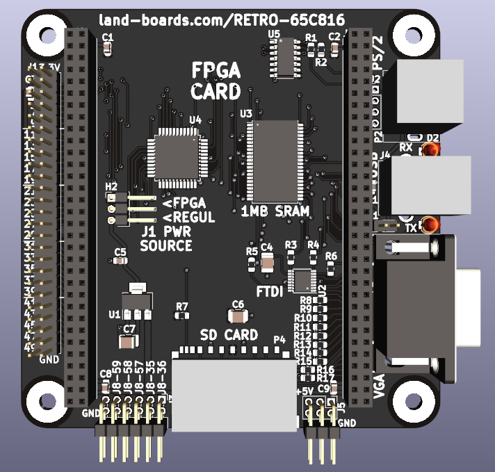
- Design based on RETRO-EP4CE15 card
- Adds 65C816 CPU
- 5V level translator for keyboard
- 5V header moved to board edge
- 65C816 CPU
- 3.3V
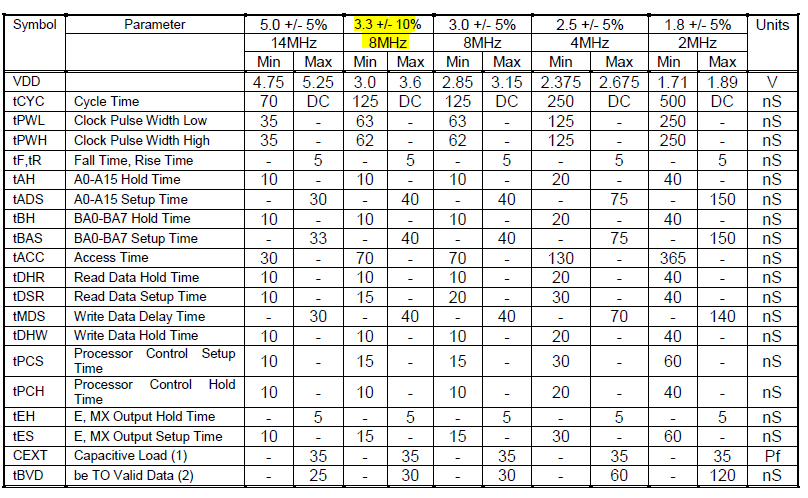
- 8 MHz
- All pins are brought to FPGA
- Address A0-A15 and Data lines also go directly to the SRAM
- FPGA can have the ROM internally or download it to the SRAM
- 1MB SRAM
- 45nS access time
- USB B
- FTDI USB to TTL
- Tx/Rx LEDs
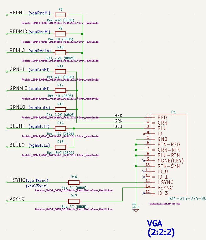
- VGA
- 3:3:2 R:G:B
- PS/2 keyboard
- 5V KEYBOARD
- Level translator to 3.3V for FPGA
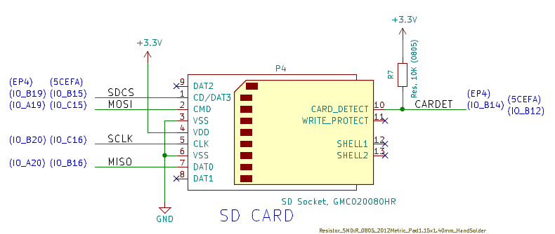
- SD card socket
- Full-sized SD
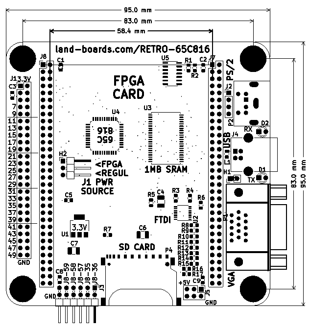
- QMTECH FPGA card mounts on top
- 95x95mm card
- ODAS form factor
- (4) 6-32 Mounting holes
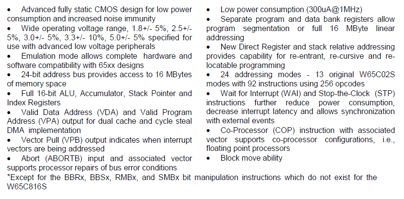
65C816 CPU
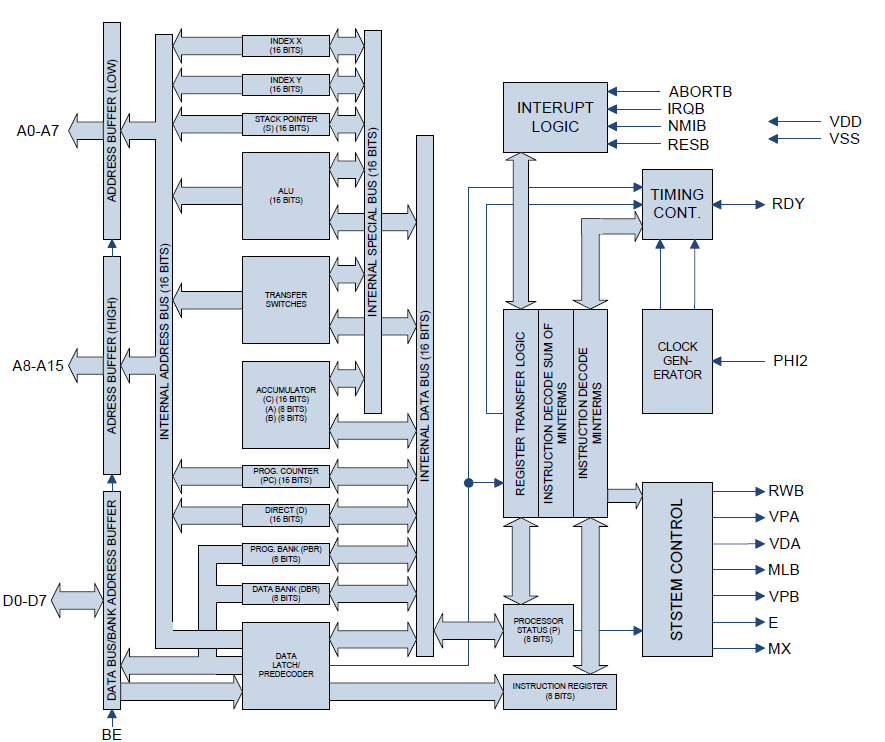
Block Diagram
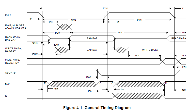
Timing
Connectors
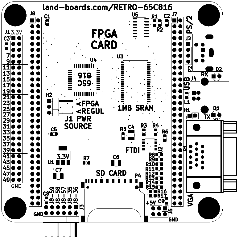
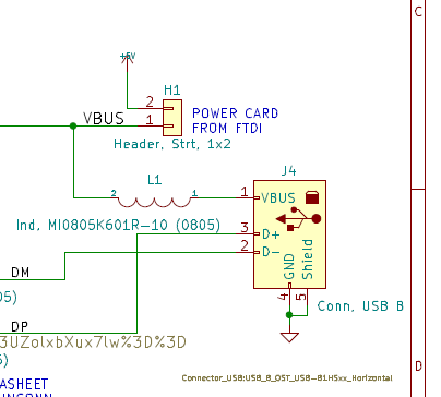
H1 - 5V
- Install jumper to power card from USB
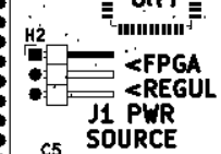
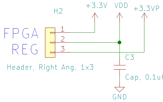
H2 - VREG I/O Conn
- Power to J1
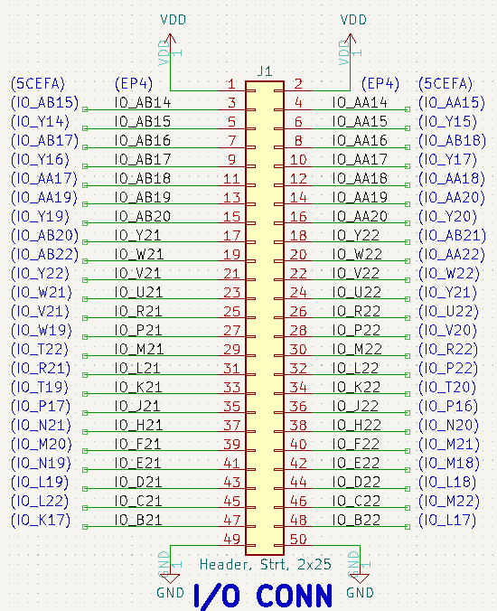
J1 - I/O Connector
- 50-pin I/O Connector
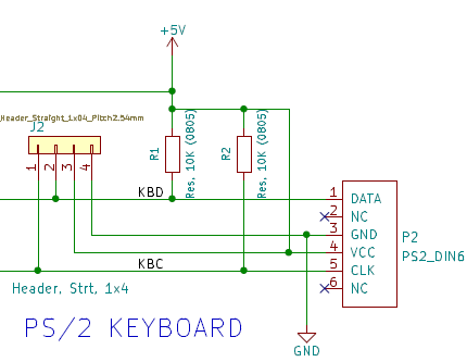
J2 - Keyboard
- 1x4 header
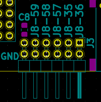
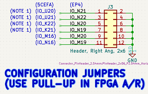
J3 - 6 FPGA pins
J4 - USB B Serial/Power
- Serial to/from FTDI
- Can power the card
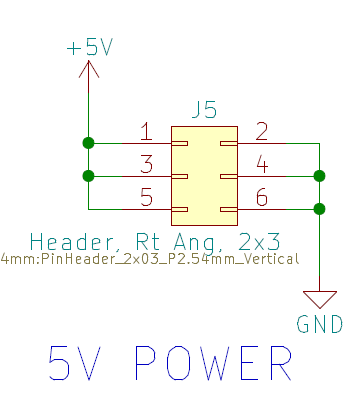
J5 - 5V/GND
- 5V/ground for external 5V logic
J7 Pin Mapping Card to FPGA pins - Right connector
| U7 PIN | EP4CE15 | EP4CE55 | 5CEFA2 | CYC 10 | FUNCTION | U7 PIN | EP4CE15 | EP4CE55 | 5CEFA2 | CYC 10 | FUNCTION | |
|---|---|---|---|---|---|---|---|---|---|---|---|---|
| 1 | GND | GND | GND | GND | GND | 2 | GND | GND | GND | GND | GND | |
| 3 | 3.3V | 3.3V | 3.3V | 3.3V | 3.3V | 4 | 3.3V | 3.3V | 3.3V | 3.3V | 3.3V | |
| 5 | GND | GND | GND | GND | GND | 6 | GND | GND | GND | GND | GND | |
| 7 | PIN_R1 | PIN_R1 | PIN_AA2 | PIN_G1 | PS2CLK | 8 | PIN_R2 | PIN_R2 | PIN_AA1 | PIN_G2 | PS2DAT | |
| 9 | PIN_P1 | PIN_P1 | PIN_Y3 | PIN_D1 | SRAMA4 | 10 | PIN_P2 | PIN_P2 | PIN_W2 | PIN_C2 | SRAMA5 | |
| 11 | PIN_N1 | PIN_N1 | PIN_U1 | PIN_B1 | SRAMA3 | 12 | PIN_N2 | PIN_N2 | PIN_U2 | PIN_F5 | SRAMA6 | |
| 13 | PIN_M1 | PIN_M1 | PIN_N1 | PIN_D3 | SRAMA2 | 14 | PIN_M2 | PIN_M2 | PIN_N2 | PIN_C3 | SRAMA7 | |
| 15 | PIN_J1 | PIN_J1 | PIN_L1 | PIN_B3 | SRAMA1 | 16 | PIN_J2 | PIN_J2 | PIN_L2 | PIN_A3 | SRAM0E_N | |
| 17 | PIN_H1 | PIN_H1 | PIN_G1 | PIN_B4 | SRAMA0 | 18 | PIN_H2 | PIN_H2 | PIN_G2 | PIN_A4 | SRAMA8 | |
| 19 | PIN_F1 | PIN_F1 | PIN_E2 | PIN_E5 | SRAMCS_N | 20 | PIN_F2 | PIN_F2 | PIN_D3 | PIN_A2 | SRAMD7 | |
| 21 | PIN_E1 | PIN_E1 | PIN_C1 | PIN_D4 | SRAMD0 | 22 | PIN_D2 | PIN_D2 | PIN_C2 | PIN_E6 | SRAMD6 | |
| 23 | PIN_C1 | PIN_C1 | PIN_G6 | PIN_C6 | SRAMD1 | 24 | PIN_C2 | PIN_C2 | PIN_H6 | PIN_D6 | SRAMD5 | |
| 25 | PIN_B1 | PIN_B1 | PIN_G8 | PIN_B5 | SRAMD2 | 26 | PIN_B2 | PIN_B2 | PIN_H8 | PIN_A5 | SRAMD4 | |
| 27 | PIN_B3 | PIN_B3 | PIN_F7 | PIN_B6 | SRAMD3 | 28 | PIN_A3 | PIN_A3 | PIN_E7 | PIN_A6 | SRAMA9 | |
| 29 | PIN_B4 | PIN_B4 | PIN_D6 | PIN_B7 | SRAMWE_N | 30 | PIN_A4 | PIN_A4 | PIN_C6 | PIN_A7 | SRAMA10 | |
| 31 | PIN_C4 | PIN_C4 | PIN_E9 | PIN_D8 | SRAMA19 | 32 | PIN_C3 | PIN_C3 | PIN_D9 | PIN_C8 | SRAMA11 | |
| 33 | PIN_B5 | PIN_B5 | PIN_B5 | PIN_D9 | SRAMA18 | 34 | PIN_A5 | PIN_A5 | PIN_A5 | PIN_C9 | SRAMA12 | |
| 35 | PIN_B6 | PIN_B6 | PIN_B6 | PIN_B8 | SRAMA17 | 36 | PIN_A6 | PIN_A6 | PIN_B7 | PIN_A8 | SRAMA13 | |
| 37 | PIN_B7 | PIN_B7 | PIN_A7 | PIN_B9 | SRAMA16 | 38 | PIN_A7 | PIN_A7 | PIN_A8 | PIN_A9 | SRAMA14 | |
| 39 | PIN_B8 | PIN_B8 | PIN_A9 | PIN_E9 | N/C | 40 | PIN_A8 | PIN_A8 | PIN_A10 | PIN_E8 | SRAMA15 | |
| 41 | PIN_B9 | PIN_B9 | PIN_B10 | PIN_E11 | CARDDET | 42 | PIN_A9 | PIN_A9 | PIN_C9 | PIN_E10 | N/C | |
| 43 | PIN_B10 | PIN_B10 | PIN_G10 | PIN_A10 | USBRX/o_FPGATX | 44 | PIN_A10 | PIN_A10 | PIN_F10 | PIN_B10 | USBCTS/o_FPGARTS | |
| 45 | PIN_B13 | PIN_B13 | PIN_C11 | PIN_D12 | USBTX/i_FPGARX | 46 | PIN_A13 | PIN_A13 | PIN_B11 | PIN_D11 | UBSRTS/i_FPGACTS | |
| 47 | PIN_B14 | PIN_B14 | PIN_B12 | PIN_B11 | REDHI | 48 | PIN_A14 | PIN_A14 | PIN_A12 | PIN_A11 | REDMID | |
| 49 | PIN_B15 | PIN_B15 | PIN_E12 | PIN_B12 | REDLO | 50 | PIN_A15 | PIN_A15 | PIN_D12 | PIN_A12 | GRNHI | |
| 51 | PIN_B16 | PIN_B16 | PIN_D13 | PIN_B13 | GRNMID | 52 | PIN_A16 | PIN_A16 | PIN_C13 | PIN_A13 | GRNLO | |
| 53 | PIN_B17 | PIN_B17 | PIN_B13 | PIN_B14 | BLUHI | 54 | PIN_A17 | PIN_A17 | PIN_A13 | PIN_A14 | BLULO | |
| 55 | PIN_B18 | PIN_B18 | PIN_A15 | PIN_D14 | HSYNC | 56 | PIN_A18 | PIN_A18 | PIN_A14 | PIN_C14 | VSYNC | |
| 57 | PIN_B19 | PIN_B19 | PIN_B15 | PIN_B16 | SDCS_N | 58 | PIN_A19 | PIN_A19 | PIN_C15 | PIN_A15 | SD_MOSI | |
| 59 | PIN_B20 | PIN_B20 | PIN_C16 | PIN_C16 | SD_SCK | 60 | PIN_A20 | PIN_A20 | PIN_B16 | PIN_C15 | SD_MISO | |
| 61 | GND | GND | GND | GND | GND | 62 | GND | GND | GND | GND | GND | |
| 63 | VIN | VIN | VIN | VIN | VIN | 64 | VIN | VIN | VIN | VIN | VIN |
J8 Pin Mapping Card to FPGA pins - Left connector
- Cyclone 10 notes
- Cannot place output or bidirectional pin J8IO[35] in input pin location M16
- Cannot place output or bidirectional pin J8IO[36] in input pin location M15
- Cannot place output or bidirectional pin J8IO[57] in input pin location E16
- Cannot place output or bidirectional pin J8IO[58] in input pin location E15
| U8 PIN | EP4CE15 | EP4CE55 | 5CEFA2 | 10C1006 | J1 | Function | U8 PIN | EP4CE15 | EP4CE55 | 5CEFA2 | 10C1006 | J1 | Function | |
|---|---|---|---|---|---|---|---|---|---|---|---|---|---|---|
| 1 | GND | GND | GND | GND | N/C | 2 | GND | GND | GND | GND | N/C | |||
| 3 | 3.3V | 3.3V | 3.3V | 3.3V | J1-1 | 4 | 3.3V | 3.3V | 3.3V | 3.3V | J1-2 | |||
| 5 | GND | GND | GND | GND | N/C | 6 | GND | GND | GND | GND | N/C | |||
| 7 | PIN_AA13 | PIN_AA13 | PIN_AA14 | PIN_R9 | N/C | CPUE | 8 | PIN_AB13 | PIN_AB13 | PIN_AA13 | PIN_T9 | N/C | CPURES* | |
| 9 | PIN_AA14 | PIN_AA14 | PIN_AA15 | PIN_R10 | J1-4 | CPUMX | 10 | PIN_AB14 | PIN_AB14 | PIN_AB15 | PIN_T10 | J1-3 | CPUCLK | |
| 11 | PIN_AA15 | PIN_AA15 | PIN_Y15 | PIN_R11 | J1-6 | CPUBE | 12 | PIN_AB15 | PIN_AB15 | PIN_Y13 | PIN_T11 | J1-5 | CPUNMIB | |
| 13 | PIN_AA16 | PIN_AA16 | PIN_AB18 | PIN_R12 | J1-8 | CPURWB | 14 | PIN_AB16 | PIN_AB16 | PIN_AB17 | PIN_T12 | J1-7 | CPUIRQB | |
| 15 | PIN_AA17 | PIN_AA17 | PIN_Y7 | PIN_N9 | J1-10 | CPUVDA | 16 | PIN_AB17 | PIN_AB17 | PIN_Y16 | PIN_M9 | J1-9 | CPUABORTB | |
| 17 | PIN_AA18 | PIN_AA18 | PIN_AA18 | PIN_M10 | J1-12 | CPUVPA | 18 | PIN_AB18 | PIN_AB18 | PIN_AA17 | PIN_P9 | J1-11 | CPURDY | |
| 19 | PIN_AA19 | PIN_AA19 | PIN_AA20 | PIN_P11 | J1-14 | CPUVPB | 20 | PIN_AB19 | PIN_AB19 | PIN_AA19 | PIN_N11 | J1-13 | CPUMLB | |
| 21 | PIN_AA20 | PIN_AA20 | PIN_Y20 | PIN_R13 | I1-16 | 22 | PIN_AB20 | PIN_AB20 | PIN_Y19 | PIN_T13 | J1-15 | |||
| 23 | PIN_Y22 | PIN_Y22 | PIN_AB21 | PIN_T15 | J1-18 | 24 | PIN_Y21 | PIN_Y21 | PIN_AB20 | PIN_T14 | J1-17 | |||
| 25 | PIN_W22 | PIN_W22 | PIN_AA22 | PIN_N12 | J1-20 | 26 | PIN_W21 | PIN_W21 | PIN_AB22 | PIN_M11 | J1-19 | |||
| 27 | PIN_V22 | PIN_V22 | PIN_W22 | PIN_R14 | J1-22 | 28 | PIN_V21 | PIN_V21 | PIN_Y22 | PIN_N13 | J1-21 | |||
| 29 | PIN_U22 | PIN_U22 | PIN_Y21 | PIN_N14 | J1-24 | 30 | PIN_U21 | PIN_U21 | PIN_W21 | PIN_P14 | J1-23 | |||
| 31 | PIN_R22 | PIN_R22 | PIN_U22 | PIN_P16 | J1-26 | 32 | PIN_R21 | PIN_R21 | PIN_V21 | PIN_R16 | J1-25 | |||
| 33 | PIN_P22 | PIN_P22 | PIN_V20 | PIN_N16 | J1-28 | 34 | PIN_P21 | PIN_P21 | PIN_W19 | PIN_N15 | J1-27 | |||
| 35 | PIN_N22 | PIN_N22 | PIN_U21 | PIN_M16 (Note) | J3-3 | 36 | PIN_N21 | PIN_N21 | PIN_U20 | PIN_M15 (Note) | J3-1 | |||
| 37 | PIN_M22 | PIN_M22 | PIN_R22 | PIN_L16 | J1-30 | 38 | PIN_M21 | PIN_M21 | PIN_T22 | PIN_L15 | J1-29 | |||
| 39 | PIN_L22 | PIN_L22 | PIN_P22 | PIN_P15 | J1-32 | 40 | PIN_L21 | PIN_L21 | PIN_R21 | PIN_M12 | J1-31 | |||
| 41 | PIN_K22 | PIN_K22 | PIN_T20 | PIN_L14 | J1-34 | 42 | PIN_K21 | PIN_K21 | PIN_T19 | PIN_L13 | J1-33 | |||
| 43 | PIN_J22 | PIN_J22 | PIN_P16 | PIN_K16 | J1-36 | 44 | PIN_J21 | PIN_J21 | PIN_P17 | PIN_K15 | J1-35 | |||
| 45 | PIN_H22 | PIN_H22 | PIN_N20 | PIN_K12 | J1-38 | 46 | PIN_H21 | PIN_H21 | PIN_N21 | PIN_J12 | J1-37 | |||
| 47 | PIN_F22 | PIN_F22 | PIN_M21 | PIN_J14 | J1-40 | 48 | PIN_F21 | PIN_F21 | PIN_M20 | PIN_J13 | J1-39 | |||
| 49 | PIN_E22 | PIN_E22 | PIN_M18 | PIN_K11 | J1-42 | 50 | PIN_E21 | PIN_E21 | PIN_N19 | PIN_J11 | J1-41 | |||
| 51 | PIN_D22 | PIN_D22 | PIN_L18 | PIN_G11 | J1-44 | 52 | PIN_D21 | PIN_D21 | PIN_L19 | PIN_F11 | J1-43 | |||
| 53 | PIN_C22 | PIN_C22 | PIN_M22 | PIN_F13 | J1-46 | 54 | PIN_C21 | PIN_C21 | PIN_L22 | PIN_F14 | J1-45 | |||
| 55 | PIN_B22 | PIN_B22 | PIN_L17 | PIN_F10 | J1-48 | 56 | PIN_B21 | PIN_B21 | PIN_K17 | PIN_F9 | J1-47 | |||
| 57 | PIN_N20 | PIN_N20 | PIN_K22 | PIN_E16 (Note) | J3-5 | 58 | PIN_N19 | PIN_N19 | PIN_K21 | PIN_E15 (Note) | J3-7 | |||
| 59 | PIN_M20 | PIN_M20 | PIN_M16 | PIN_D16 | J3-8 | 60 | PIN_M19 | PIN_M19 | PIN_N16 | PIN_D15 | J3-11 | |||
| 61 | GND | GND | GND | GND | J1-50 | 62 | GND | GND | GND | GND | J1-49 | |||
| 63 | +5V | +5V | +5V | +5V | J1-50 | 64 | +5V | +5V | +5V | +5V | J1-50 |
P1 - VGA
- DB-15HD connector
- 3:3:2 R:G:B
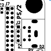
P2 - PS/2 Keyboard
- Purple DIN-6 for PS/2 keyboard
P4 - SD Card
Mechanicals
MultiComp On RETRO-65C816 VHDL Code
References/Notes
- On the usefulness of 65816 as a 65C02 alternative
- Helpful timing information
...potential for data bus contention during Ø2 low. My solution was two-fold: use VDA and VPA to qualify chip selects, and qualify read-accesses with Ø2. The former assures that an addressed device will not respond to selection until the address bus is truly valid—invalid bus states may occur during the execution of some instructions. The latter assures that a selected device will not drive the data bus when the '816 is presenting A16-A23 on it. This solution doesn't totally eliminate the risk of contention but greatly narrows the window of opportunity for it. The need for more stringent qualifying of D0-D7 would depend on the peripheral silicon on the bus. In the case of POC and the Ø2 rate I'm using (12.5 MHz maximum), everything gets off the data bus before the '816 starts to drive it with the bank address. That would not be the case if I were to increase Ø2 to 20 MHz, however.

Floating the buses with BE creates the odd situation where no valid address exists on A0-A15, which I daresay could cause a device to be selected solely because of a residual charge in bus capacitance. Also, BE floats the RWB signal*, which may trip up other logic that is dependent on RWB always being driven to one state or the other. The most fool-proof solution is the use of a data bus transceiver as you suggested, which is a straightforward method (74AC245 or 74AHC245 recommended if Ø2 will exceed 8 MHz).
Revision History
Rev 2
- Fixed W65C816 footprint
- Bigger footprint
- Moved around a lot of tracks to remove ground trace and use ground plane
- Changed from 2:2:2 to 3:3:2 bit video (256 colors)
- Changed J1 pinout to not use 2 input-only J8 pins
- Shuffled J7 pinout
Rev 1
- W65C816 footprint is too small for part
- Used TQFP footprint but part is clearly too big
- Datasheet does not indicate package detail
- 0.8mm pitch was OK
- Works well as RETRO-EP4CE15 replacement
- PS/2 @5V is good
Videos
- 65C816 Computer 27 Videos Series - Adrien Kohlbecker
- Lot of detail on 65C816 hardware
