Difference between revisions of "LB-6809-01"
Jump to navigation
Jump to search
Blwikiadmin (talk | contribs) |
Blwikiadmin (talk | contribs) |
||
| Line 14: | Line 14: | ||
* 0x8000-0x9FFF Free Space (8KB) | * 0x8000-0x9FFF Free Space (8KB) | ||
* 0xA000-0xBFFF Serial (ACIA) | * 0xA000-0xBFFF Serial (ACIA) | ||
| − | * 0xC000- | + | * 0xC000-0xFFFF 16KB EPROM |
== Design == | == Design == | ||
Revision as of 12:32, 21 August 2024
Contents
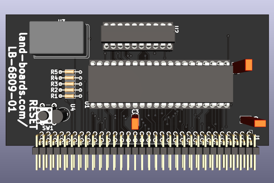
Features
- 68B09 CPU
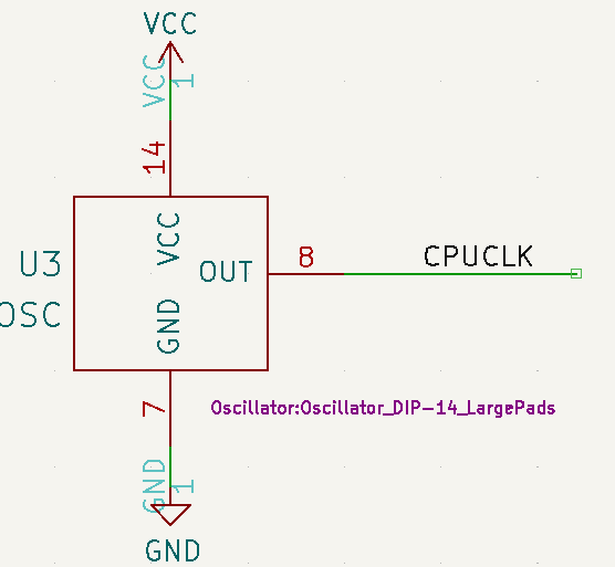
- 2 MHz (typical) Oscillator on card
- Reset switch/power monitor
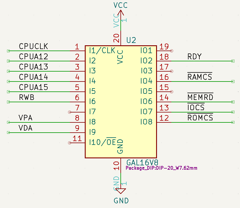
- Address decoder PLD drives RAM/ROM/IO chip selects
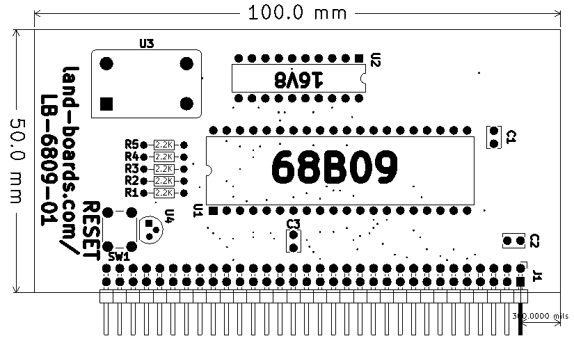
- 100x50mm card
Memory Map
- 0x0000-0x7FFF 32KB SRAM
- 0x8000-0x9FFF Free Space (8KB)
- 0xA000-0xBFFF Serial (ACIA)
- 0xC000-0xFFFF 16KB EPROM
Design
68B09 CPU
Oscillator
PLD
PLD Listing
Name       LB-6809-01_PLD;
Partno     ATF16V8B;
Date       08/19/24;
Revision   01;
Designer   DOUG G;
Company    LAND BOARDS LLC;
Assembly   LB680901_U2;
Location   Rustbelt, US;
Device     G16V8;

/*
*/


/* Control inputs */
PIN    1   = CLK;
PIN    2   = CPUA12;
PIN    3   = CPUA13;
PIN    4   = CPUA14;
PIN    5   = CPUA15;
PIN    6   = CPUREAD;
PIN    7   = VPB;		/* Added as wire on Rev 1 PCB	*/
PIN    8   = VPA;
PIN    9   = VDA;

/* Address Decode and Chip Select outputs */
PIN    12  = !ROMCS;
PIN    13  = !IOCS;
PIN    14  = !MEMRD;
PIN    16  = !RAMCS;
PIN    18  = RDY;

ROMCS = CPUA15 & CPUA14 & VPB;

RAMCS = !CPUA15 & VPB
#        CPUA15 & !CPUA14 & !CPUA13 & VPB;

IOCS = CPUA15 & !CPUA14 & CPUA13 & VPB;

RDY = VPB;

MEMRD = CPUREAD & VPB;
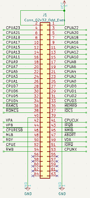
Backplane connector
Mechanicals
Checkout
Rev 1 Checkout Notes
- Add wire U1-34 to U2-7 (VPB/E)
