Difference between revisions of "ESP32-VGA"
Jump to navigation
Jump to search
Blwikiadmin (talk | contribs) |
Blwikiadmin (talk | contribs) |
||
| Line 173: | Line 173: | ||
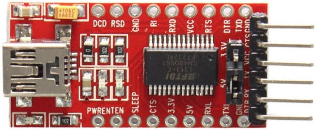
=== J6 - FTDI #2 === | === J6 - FTDI #2 === | ||
| + | |||
| + | * Set FTDI jumper to 3.3V | ||
[[File:FTDI_rot.jpg]] | [[File:FTDI_rot.jpg]] | ||
Revision as of 15:34, 1 February 2020
Contents
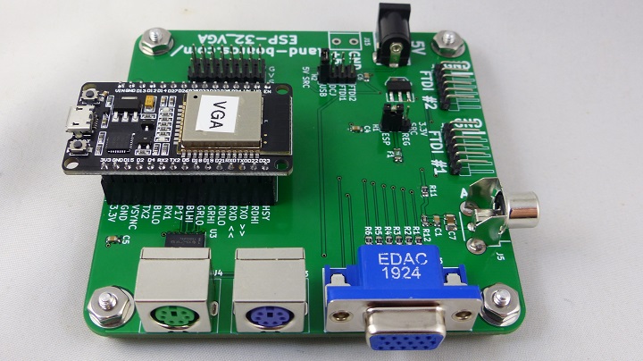
Features
- ESP32 Module
- 6-bit VGA color
- 2 x PS-2 DIN connectors
- 5V mouse/keyboard
- 3.3V to 5V level shifters
- 10K pull-ups on both sides
- 2 x FTDI connectors
- 5V DC Jack
- 3.3V regulator (optional)
- GVS pins for extra ESP32 pins
- 95x95mm form factor
- 6-32 mounting holes
ESP-32 Module
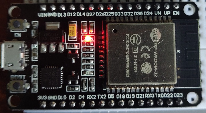
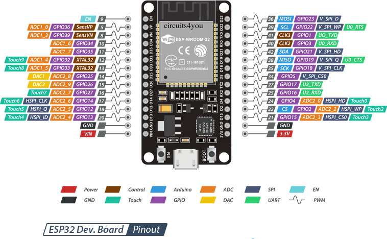
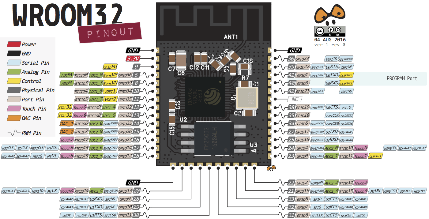
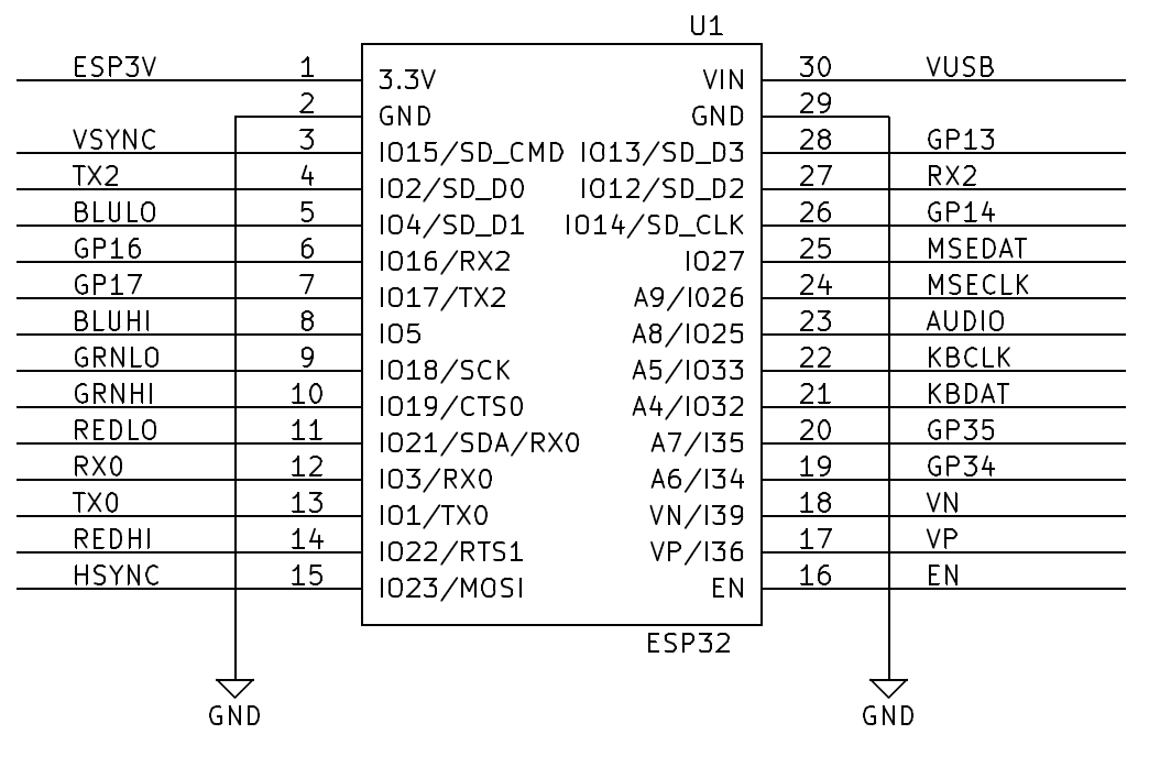
- ESP32 DevKit ESP32-WROOM GPIO Pinout
- On board Blue LED = Arduino Pin 2
Module Features
- Architecture: Xtensa Dual-Core 32-bit LX6
- CPU frequency: up to 240MHz
- Total RAM available: 528KB (part of it reserved for system)
- BootROM: 448KB
- Internal FlashROM: none
- External FlashROM: code and data, via SPI Flash; usual size 4MB
- GPIO: 34 (GPIOs are multiplexed with other functions, including external FlashROM, UART, etc.)
- UART: 3 RX/TX UART (no hardware handshaking), one TX-only UART
- SPI: 4 SPI interfaces (one used for FlashROM)
- I2C: 2 I2C (bitbang implementation available on any pins)
- I2S: 2
- ADC: 12-bit SAR ADC up to 18 channels
- DAC: 2 8-bit DACs
- RMT: 8 channels allowing accurate pulse transmit/receive
- Programming: using BootROM bootloader from UART - due to external FlashROM and always-available BootROM bootloader, the ESP32 is not brickable
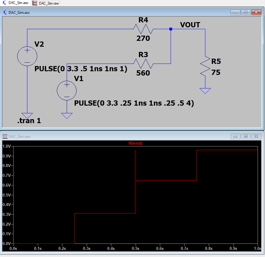
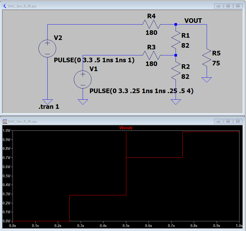
Video DAC LTSpice Simulation
- Video DAC Simulation files
- Video is 2:2:2 - R:G:B
Summing Resistor DAC - Rev 1 Board
- 5% resistors are "good enough"
- 1V into 75 Ohm VGA load
- 3.3V drive
- ESP32 has 40 mA drive
- Uses 10 mA (max)
- R4 = 1.2 mA to -10 mA
- R3 = 1.1 mA to -5.3 mA
- Output in 4 steps
- 0V
- 0.3V
- 0.65V
- 0.96V
R-2R DAC - Rev 2 Board
- 5% resistors are "good enough"
- 1V into 75 Ohm VGA load
- 3.3V drive
- ESP32 has 40 mA drive
- Uses < 15 mA (max)
- R4 = +1.6 mA to -14.4 mA
- R3 = +1.6 mA to -14.2 mA
- Output in 4 steps
- 0V
- 0.3V
- 0.7V
- 1.0V
Headers
H1 - 3.3V SRC select
- 1-2 = Get 3.3V from ESP32 on-board regulator
- 2-3 = Get 3.3V from on-board regulator (Default)
H2 - 5V SRC Select Jumper
- 2x4 header
- Care must be taken to install the correct jumpers
- USB jumper sends out 5V when a USB cable is connected to the ESP32 module
- USB jumper sends 5V into the ESP32 module when there is no USB cable connected to the ESP32 module
Power from DC Jack
- 1-2 = VUSB - Install - 5V goes to ESP (Do not attach USB cable)
- 3-4 = DCIN - Install - Power comes from DC jack
- 5-6 = FTDI5V_1 - Do not install
- 7-8 = FTDI5V_2 - Do not install
Power from USB on ESP32 module
- 1-2 = VUSB - Install - 5V comes from USB on ESP32 module
- 3-4 = DCIN - Do not install
- 5-6 = FTDI5V_1 - Do not install
- 7-8 = FTDI5V_2 - Do not install
Power from FTDI #1
- 1-2 = VUSB - Install - 5V goes to ESP (Do not attach USB cable)
- 3-4 = DCIN - Power comes from DC jack - Do not power
- 7-8 = FTDI5V_2 - Do not install
Power from FTDI #2
- 1-2 = VUSB - Install - 5V goes to ESP (Do not attach USB cable)
- 3-4 = DCIN - Power comes from DC jack - Do not power
- 5-6 = FTDI5V_1 - Do not install
- 7-8 = FTDI5V_2 - Install
Connectors
P3/P4 = GVS
- GP13
- GP14
- GP16
- GP17
- GP35
- GP23
- VN
- VP
P3 - VGA
J3 - PS/2 Keyboard
- Purple DIN 6 connector
J4 - PS/2 Mouse
- DIN 6 connector
J2 - FTDI #1
- Set FTDI jumper to 3.3V
- GND
- RTS (Not used)
- 5V (Power in if H2 is configured)
- RX (from card to External FTDI)
- TX (from External FTDI to card)
- CTS (Not used)
J6 - FTDI #2
- Set FTDI jumper to 3.3V
- GND
- RTS (Not used)
- 5V (Power in if H2 is configured)
- RX (from card to External FTDI)
- TX (from External FTDI to card)
- CTS (Not used)
J5 - Audio Out - RCA Jack
FabGL GPIOs assignment summary - fabgl dev board rev2
P3 - VGA
  HSync => 23
  VSync => 15
  R0    => 22
  R1    => 21
  G0    => 19
  G1    => 18
  B0    => 5
  B1    => 4
PS/2 - Keyboard
  DAT   => 32
  CLK   => 33
PS/2 - Mouse
  DAT   => 27
  CLK   => 26
Audio
AUD => 25
SDCard - HSPI
- Brought to GVS header pins
  MOSI  => 17
  MISO  => 16
  CLK   => 14
  CS    => 13
UART - UART2
  RX    => 34
  TX    => 2
I2C (not usable with VGA)
  SDA   => 4  (conflicts with VGA B1)
  SCL   => 15 (conflicts with VGA VSync)
SPI Display - VSPI (not usable with VGA)
  CLK   => 18 (conflicts with VGA G1)
  MISO  => 19 (conflicts with VGA G0)
  MOSI  => 23 (conflicts with VGA HSync)
  CS    => 5  (conflicts with VGA B0)
  D/C   => 22 (conflicts with VGA R0)
  RESET => 21 (conflicts with VGA R1)
Software
FabGL
Display Controller (VGA, SSD1306), PS/2 Mouse and Keyboard Controller, Graphics Library, Sound Engine, Game Engine and ANSI/VT Terminal for the ESP32
- FabGL - ESP32 Display Controller and Graphics Library
- FabGL Github repo
MicroPython
- MicroPython Homepage
- GitHub repo (MicroPython)
ESP-IDF
Operating Systems
- FreeRTOS
- ESP32 DevKit v1
- LuaNode
- ESP32 DEVKITV1 module schematics (also helpful discussion)
Arduino Programming
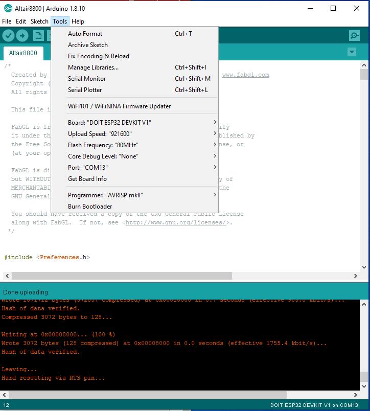
- Board : "DOIT ESP32 DEVKIT V1"
Schematic
Prototype
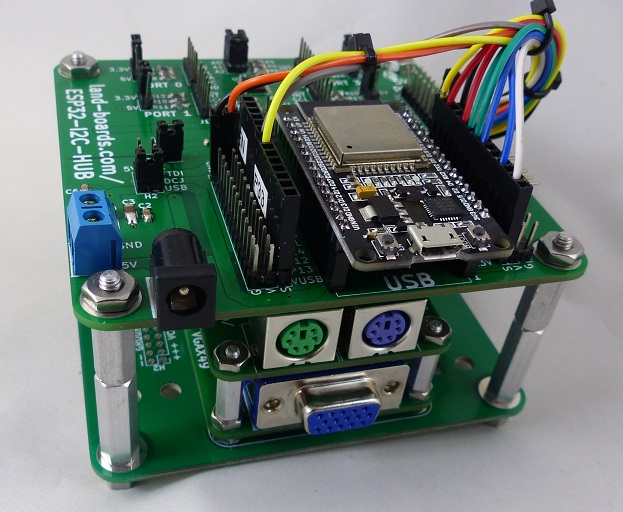
- ESP32-I2C-HUB
- VGAX49
- PS2X49
- Purple = Keyboard
- Green = Mouse
- 95mm to 49mm Adapter card
- 6-32/4-40 Standoffs, screws, nuts
- Cabling

