Difference between revisions of "VGAX49"
Jump to navigation
Jump to search
Blwikiadmin (talk | contribs) |
Blwikiadmin (talk | contribs) |
||
| Line 24: | Line 24: | ||
=== 2:2:2 Resistor Simulation === | === 2:2:2 Resistor Simulation === | ||
| − | * 3.3V Drive | + | * 3.3V Drive out of FPGA |
| + | * 1V is drive level for VGA specification | ||
* 8 mA max drive current | * 8 mA max drive current | ||
* VGA presents a 75 Ohm load | * VGA presents a 75 Ohm load | ||
| Line 30: | Line 31: | ||
=== 5:6:5 Resistor Simulation === | === 5:6:5 Resistor Simulation === | ||
| − | * 3.3V Drive | + | * 3.3V Drive out of FPGA |
| + | * 1V is drive level for VGA specification | ||
* 8 mA max drive current | * 8 mA max drive current | ||
* VGA presents a 75 Ohm load | * VGA presents a 75 Ohm load | ||
Revision as of 17:54, 13 February 2020
Contents
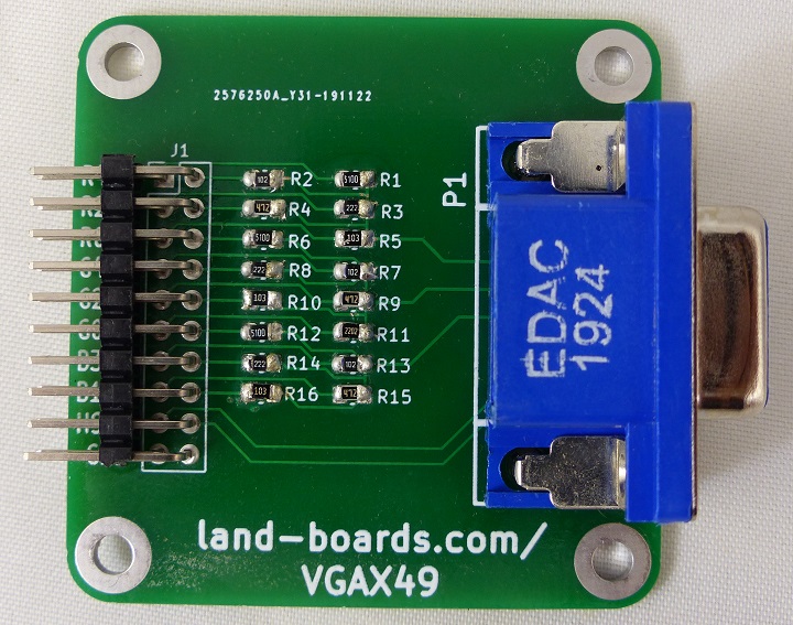
Features
- Digital VGA adapter
- 16-bit digital video
- 5:6:5 (R:G:B) mapping (maximum)
- 2:2:2 (R:G:B) mapping (option)
- Uses summing resistors
- DB-15F connector
- 49x49mm ODAS form factor
- Mounting holes
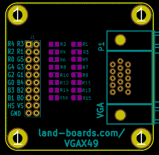
Connectors
J1 - Digital Connections
P1 - VGA connector
Simulation
2:2:2 Resistor Simulation
- 3.3V Drive out of FPGA
- 1V is drive level for VGA specification
- 8 mA max drive current
- VGA presents a 75 Ohm load
5:6:5 Resistor Simulation
- 3.3V Drive out of FPGA
- 1V is drive level for VGA specification
- 8 mA max drive current
- VGA presents a 75 Ohm load

