Difference between revisions of "QM Tech Cyclone V FPGA Board"
Jump to navigation
Jump to search
Blwikiadmin (talk | contribs) |
Blwikiadmin (talk | contribs) |
||
| Line 78: | Line 78: | ||
* sdRamData[14] = PIN_BANK_3B_R12 | * sdRamData[14] = PIN_BANK_3B_R12 | ||
* sdRamData[15] = PIN_BANK_3B_P12 | * sdRamData[15] = PIN_BANK_3B_P12 | ||
| + | == Programming the FPGA EEPROM (5CEFA2F23 FPGA) == | ||
| + | |||
| + | * File | ||
| + | * Convert Programming File | ||
| + | * Configuration Device = MT25QL128 | ||
| + | * Mode = Active Serial | ||
| + | * Programming File Type: *.jic | ||
| + | * Advanced = Check both Disables... | ||
| + | * Select Flash Loader | ||
| + | * Add Device = Cyclone V and 5CEFA2 | ||
| + | * Select SOF Data | ||
| + | * Select Add File and select the .sof file | ||
| + | * Generate | ||
| + | * In Tools, Programmer | ||
| + | * Mode: JTAG | ||
| + | * Add file and select the .jic file | ||
| + | * Select Program/Configure | ||
| + | * Takes a while to program | ||
| + | * Press button near VGA | ||
== Resources == | == Resources == | ||
* [https://github.com/ChinaQMTECH/QM_CYCLONE_V GitHub Repo] | * [https://github.com/ChinaQMTECH/QM_CYCLONE_V GitHub Repo] | ||
Revision as of 00:31, 11 August 2020
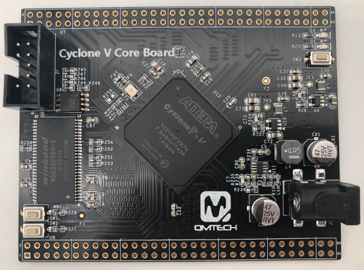
- QMTECH Altera Intel FPGA Core Board Cyclone V CycloneV 5CEFA2F23 SDRAM
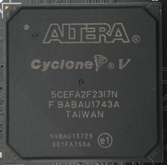
- On-Board FPGA: 5CEFA2F23I7N
- On-Board FPGA external crystal frequency: 50MHz
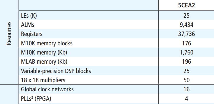
- 5CEFA2F23 has rich RAM resource up to 1,760Kb
- 5CEFA2F23 has 25K logic cells
- On-Board Micron MT25QL128A SPI Flash, 16M bytes for user configuration code
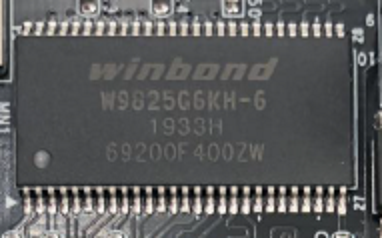
- On-Board Winbond 32MB SDRAM, W9825G6KH-6
- On-Board 3.3V power supply for FPGA by using MP2315 wide input range DC/DC
- 5CEFA2F23 core board has two 64p, 2.54mm pitch headers for extending 108 user IOs. All 108 user IOs are precisely designed with length matching
- 5CEFA2F23 core board has 3 user switches
- 5CEFA2F23 core board has 2 user LEDs
- 5CEFA2F23 core board has JTAG interface, by using 10p, 2.54mm pitch header
- 5CEFA2F23 core board PCB size is: 6.7cm x 8.4cm
- Default power source for board is: 1A@5V DC, the DC header type: DC-050, 5.5mmx2.1mm
Contents
FPGA
5CEFA2F23 FPGA Resources
- CLK_50M = PIN_BANK_3B_M9
LEDs/Switches
- Power LED = D4 (On when 5V is applied)
- User LED = LED_D5 = FPGA Pin_BANK_7A_D17
- KEY0 = SW1 = FPGA Pin_BANK_4A_AB13
- RESET_N = SW2 = FPGA PIN_BANK_4A_V16
- nCONFIG = SW3 = FPGA PIN_BANK_9A_A4
- JP5 - 5V
SDRAM
SDRAM Pins
- sdRamClk = PIN_BANK_3B_AB11
- sdRamClkEn = PIN_BANK_3B_V9
- n_sdRamCas = PIN_BANK_3B_AA7
- n_sdRamCe = PIN_BANK_3B_AB5
- n_sdRamRas = PIN_BANK_3B_AB6
- n_sdRamWe = PIN_BANK_3A_W9
- sdRamAddr[0] = PIN_BANK_3B_P8
- sdRamAddr[1] = PIN_BANK_3A_P7
- sdRamAddr[2] = PIN_BANK_3B_N8
- sdRamAddr[3] = PIN_BANK_3A_N6
- sdRamAddr[4] = PIN_BANK_3A_U6
- sdRamAddr[5] = PIN_BANK_3A_U7
- sdRamAddr[6] = PIN_BANK_3A_V6
- sdRamAddr[7] = PIN_BANK_3A_U8
- sdRamAddr[8] = PIN_BANK_3A_T8
- sdRamAddr[9] = PIN_BANK_3A_W8
- sdRamAddr[10] = PIN_BANK_3A_R6
- sdRamAddr[11] = PIN_BANK_3B_T9
- sdRamAddr[12] = PIN_BANK_3B_Y9
- sdRamAddr[13] = PIN_BANK_3A_T7
- sdRamAddr[14] = PIN_BANK_3B_P9
- sdRamData[0] = PIN_BANK_3B_AA12
- sdRamData[1] = PIN_BANK_3B_Y11
- sdRamData[2] = PIN_BANK_3B_AA10
- sdRamData[3] = PIN_BANK_3B_AB10
- sdRamData[4] = PIN_BANK_3B_Y10
- sdRamData[5] = PIN_BANK_3B_AA9
- sdRamData[6] = PIN_BANK_3B_AB8
- sdRamData[7] = PIN_BANK_3B_AA8
- sdRamData[8] = PIN_BANK_3B_U10
- sdRamData[9] = PIN_BANK_3B_T10
- sdRamData[10] = PIN_BANK_3B_U11
- sdRamData[11] = PIN_BANK_3B_R10
- sdRamData[12] = PIN_BANK_3B_R11
- sdRamData[13] = PIN_BANK_3B_U12
- sdRamData[14] = PIN_BANK_3B_R12
- sdRamData[15] = PIN_BANK_3B_P12
Programming the FPGA EEPROM (5CEFA2F23 FPGA)
- File
- Convert Programming File
- Configuration Device = MT25QL128
- Mode = Active Serial
- Programming File Type: *.jic
- Advanced = Check both Disables...
- Select Flash Loader
- Add Device = Cyclone V and 5CEFA2
- Select SOF Data
- Select Add File and select the .sof file
- Generate
- In Tools, Programmer
- Mode: JTAG
- Add file and select the .jic file
- Select Program/Configure
- Takes a while to program
- Press button near VGA


