Difference between revisions of "BLACK-PILL-HUB"
Jump to navigation
Jump to search
Blwikiadmin (talk | contribs) |
Blwikiadmin (talk | contribs) |
||
| Line 46: | Line 46: | ||
=== P2 - Vbattery === | === P2 - Vbattery === | ||
| − | * Battery power to the | + | * Battery power to the Black Pill board |
# GND | # GND | ||
# Vbat | # Vbat | ||
Revision as of 11:48, 26 January 2021
Contents
Features
- Carrier for the STM32 Black Pill Board
- STM32F401/411 CPU
- AliExpress listing
- I2C Hub - PCA9544A
- 4-channel
- Independent 3.3V/5V power for each channel
- Separate interrupts for each channel
- GVS connections for Black Pill pins
- Reset switch
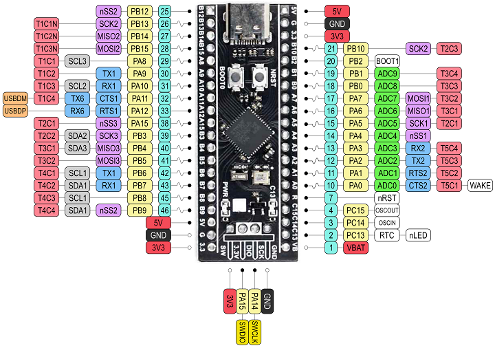
Black Pill Module
Not pin compatible with Blue Pill due to power pin locations
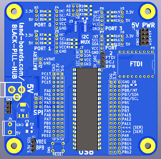
Connectors
J1 - 5V power
- DC jack
- 5V
- Center positive
J4 - 5V Power
- 5mm terminal block
J7 - I2C
- The I2C interface that goes to the I2C hub part
- SCL (PB6)
- SDA (PB7)
- 3.3V
- GND
P1 - 5V
- 2x4 header with 5V from H2 (Rev 4 card)
P2 - Vbattery
- Battery power to the Black Pill board
- GND
- Vbat
P3 - FTDI connector (Rev X1-X3)
- To cable to FTDI wires swap pins 4 and 5 in cable
- FTDI card jumper has to be set to 3.3V since STM32 has 3.3V signal levels
- GND
- N/C
- VCC (to H8 pin 2)
- TX (to Blue Pill RX) (PA10 pin on STM32)
- RX (to Blue Pill Tx) (PA9 pin on STM32)
- RESET*
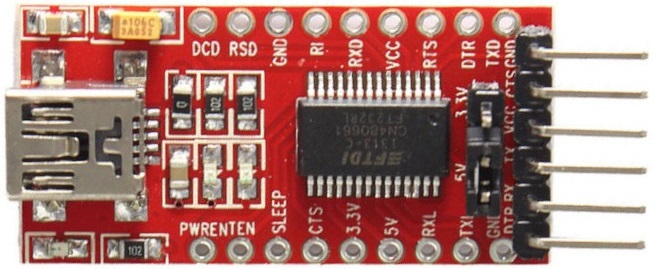
P3 - FTDI Module (Rev 4 or higher)
- Cheap FT232 module pinout
P4, P5, P6, P7 - I2C Interfaces #0-#3
- INT*
- SCL
- SDA
- VCC
- GND
P8 - SPI
- PA6 (MISO)
- 3.3V
- PA5 (SCK)
- PA7 (MOSI)
- RES
- GND
P11/P12 - GVS Connector
- Ground, Power, Signal pins
- n/c
- PC13
- PC14
- PC15
- PA0
- PA1
- PA2
- PA3
- PA4
- PA5/SCK1
- PA6/MISO1
- PA7/MOSI1
- PB0
- PB1
- PB10
- PB11
P12/P13 - GVS Connector
- Ground, Power, Signal pins
- n/c
- PB9
- I2C_INT (PB8)
- I2C_SDA1 (PB7)
- I2C_SCL (PB6)
- PB5
- PB4
- PB3
- PA15
- PA12
- PA11
- RX
- TX
- PA8
- PB15
- PB14
- PB13
- PB12
Headers
H1 - 3.3V (Rev X1-X3)
- Install to power 3.3V from regulator
H1 - 3.3V source select
- 1-2 power from 5V to 3.3V regulator
- 2-3 Power from Blue Pill board 3.3V regulator
H2 - 5V Jumper (Rev X1-X3)
- Install to connect J4 and J1 5V
H2 - 5V Power Source (Rev 4 or higher)
- T-shaped header
- Up - Power 5V from BluePill Hub USB power
- Left - Power 5V from DC Jack
- Down - Power 5V from FTDI 5V
H3, H4, H5, H6 - I2C Power
- Select the power to the I2C interface
- Install in one of the two positions to power external I2C interface from the board
- Remove if power comes in from external I2C interface
- 3.3V
- 5V
H7 - 3.3V from Blue Pill module 3.3V regulator
- Install = power on-board 3.3V circuitry from regulator on Blue Pill module
- H8 should not be installed if H7 is installed
H8 - Power from FTDI
- 1-2 = 3.3V from FTDI (don't ever do this)
- 2-3 = 5V from FTDI (probably don't do this)
- H7 should not be installed if H8 is installed
H9 - Hub Chip Address
- Select the address of the PCA9544A I2C hub
Switches
SW1 - Reset Switch
- Press to reset Blue Pill board
SW2 - Switch on/off J1, J4 power source
Schematic
Software
Testing
Programming
- ST-LINK V2
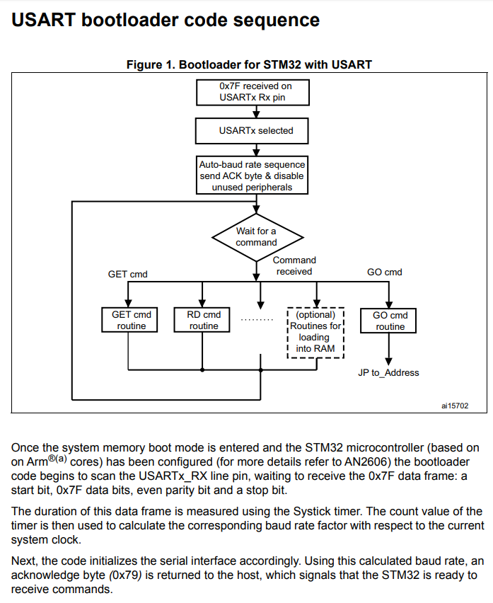
- FLASHER-STM32 - STM32 Flash loader demonstrator (UM0462)
- From AN3155


