Difference between revisions of "QMTECH Cyclone 10CL006 FPGA Card"
Jump to navigation
Jump to search
Blwikiadmin (talk | contribs) |
Blwikiadmin (talk | contribs) |
||
| Line 24: | Line 24: | ||
<pre> | <pre> | ||
| + | set_location_assignment PIN_E1 -to sys_clk | ||
| + | set_location_assignment PIN_J6 -to sys_rst_n | ||
set_location_assignment PIN_J6 -to RESET_N | set_location_assignment PIN_J6 -to RESET_N | ||
set_location_assignment PIN_L9 -to LEDR | set_location_assignment PIN_L9 -to LEDR | ||
set_location_assignment PIN_F3 -to KEY | set_location_assignment PIN_F3 -to KEY | ||
| + | # SDRAM | ||
set_location_assignment PIN_R7 -to DRAM_ADDR[0] | set_location_assignment PIN_R7 -to DRAM_ADDR[0] | ||
set_location_assignment PIN_T7 -to DRAM_ADDR[1] | set_location_assignment PIN_T7 -to DRAM_ADDR[1] | ||
Revision as of 18:15, 11 August 2021
Specification
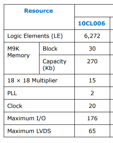
- On-Board FPGA: 10CL006YU256C8G
- On-Board FPGA external crystal frequency: 50MHz
- 10CL006YU256C8G has block RAM resource - 30 of M9K blocks
- 10CL006YU256C8G has 6K LEs
- On-Board 32MB Micron SDRAM,MT48LC16M16A2-75
- On-Board 3.3V power supply for FPGA by using MP2359 wide input range DC/DC
- QM_Cyclone10_10CL006 development board has two 64p, 2.54mm pitch headers for extending user IOs
- QM_Cyclone10_10CL006 development board has 3 user switches
- QM_Cyclone10_10CL006 development board has 2 user LEDs
- QM_Cyclone10_10CL006 development board has JTAG interface, by using 10p, 2.54mm pitch male header
- QM_Cyclone10_10CL006 development board PCB size is: 6.7cm x 8.4cm
- Default power source for board is: 1A@5V DC, the DC header type: DC-050, 5.5mmx2.1mm
- AliExpress listing
Resources
- Comparable to Cyclone IV EP4CE6 FPGA
Pin List
set_location_assignment PIN_E1 -to sys_clk
set_location_assignment PIN_J6 -to sys_rst_n
set_location_assignment PIN_J6 -to RESET_N
set_location_assignment PIN_L9 -to LEDR
set_location_assignment PIN_F3 -to KEY
# SDRAM
set_location_assignment PIN_R7 -to DRAM_ADDR[0]
set_location_assignment PIN_T7 -to DRAM_ADDR[1]
set_location_assignment PIN_R8 -to DRAM_ADDR[2]
set_location_assignment PIN_T8 -to DRAM_ADDR[3]
set_location_assignment PIN_R6 -to DRAM_ADDR[4]
set_location_assignment PIN_T5 -to DRAM_ADDR[5]
set_location_assignment PIN_R5 -to DRAM_ADDR[6]
set_location_assignment PIN_T4 -to DRAM_ADDR[7]
set_location_assignment PIN_R4 -to DRAM_ADDR[8]
set_location_assignment PIN_T3 -to DRAM_ADDR[9]
set_location_assignment PIN_T6 -to DRAM_ADDR[10]
set_location_assignment PIN_R3 -to DRAM_ADDR[11]
set_location_assignment PIN_T2 -to DRAM_ADDR[12]
set_location_assignment PIN_N8 -to DRAM_BA[0]
set_location_assignment PIN_L8 -to DRAM_BA[1]
set_location_assignment PIN_M7 -to DRAM_CAS_N
set_location_assignment PIN_R1 -to DRAM_CKE
set_location_assignment PIN_P2 -to DRAM_CLK
set_location_assignment PIN_P8 -to DRAM_CS_N
set_location_assignment PIN_N6 -to DRAM_LDQM
set_location_assignment PIN_P1 -to DRAM_UDQM
set_location_assignment PIN_M8 -to DRAM_RAS_N
set_location_assignment PIN_P6 -to DRAM_WE_N
set_location_assignment PIN_K5 -to DRAM_DQ[0]
set_location_assignment PIN_L3 -to DRAM_DQ[1]
set_location_assignment PIN_L4 -to DRAM_DQ[2]
set_location_assignment PIN_K6 -to DRAM_DQ[3]
set_location_assignment PIN_N3 -to DRAM_DQ[4]
set_location_assignment PIN_M6 -to DRAM_DQ[5]
set_location_assignment PIN_J2 -to DRAM_DQ[15]
set_location_assignment PIN_J1 -to DRAM_DQ[14]
set_location_assignment PIN_K2 -to DRAM_DQ[13]
set_location_assignment PIN_K1 -to DRAM_DQ[12]
set_location_assignment PIN_L2 -to DRAM_DQ[11]
set_location_assignment PIN_L1 -to DRAM_DQ[10]
set_location_assignment PIN_N1 -to DRAM_DQ[9]
set_location_assignment PIN_N2 -to DRAM_DQ[8]
set_location_assignment PIN_N5 -to DRAM_DQ[7]
set_location_assignment PIN_P3 -to DRAM_DQ[6]
