Difference between revisions of "BBB-GVS-3"
Jump to navigation
Jump to search
Blwikiadmin (talk | contribs) |
Blwikiadmin (talk | contribs) |
||
| Line 15: | Line 15: | ||
* Cape configuration EEPROM with write enable jumper | * Cape configuration EEPROM with write enable jumper | ||
* Beaglebone Black form factor | * Beaglebone Black form factor | ||
| + | |||
| + | == BBB-GVS-3 Assembly Sheet == | ||
| + | |||
| + | * [[BBB-GVS-3 Rev X2 Assembly Sheet]] | ||
Revision as of 19:17, 29 December 2019
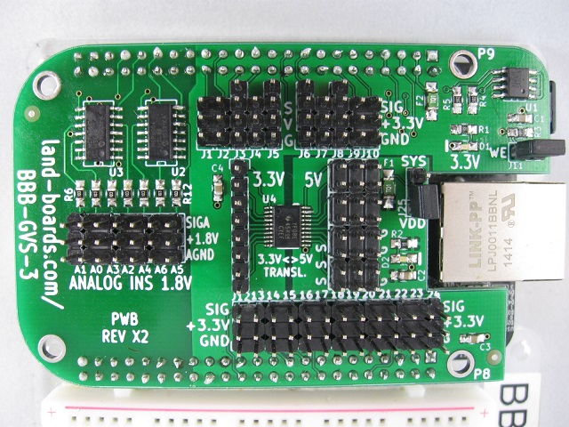
Features
- (19) GPIOs, GVS pins
- (3) UARTs, GVTxRx pins
- (1) I2C bus, GVSdaSck
- (8) Channels of 3.3V to 5V level translators
- Use female to female jumpers to route the GPIO lines to the translator channels
- 5V side has GVS pins
- (7) 1.8V analog GVS connections with analog voltage/ground
- Buffer opamps on the analog inputs
- 5V pins are all ESD protected pins with 15 kV of protection
- Selectable 5V source (SYS_5V or VDD_5V)
- Cape configuration EEPROM with write enable jumper
- Beaglebone Black form factor
