Difference between revisions of "BBB-GVS-3"
Jump to navigation
Jump to search
Blwikiadmin (talk | contribs) |
Blwikiadmin (talk | contribs) |
||
| Line 162: | Line 162: | ||
[[FILE:BBB-GVS-3_TEST_P1838_720PX.jpg]] | [[FILE:BBB-GVS-3_TEST_P1838_720PX.jpg]] | ||
| − | * Connect GRID49 card with resistor ladder | + | * Connect [[GRID49]] card with resistor ladder |
** (8) 10K resistors | ** (8) 10K resistors | ||
** From 1.8V to all 7 inputs to ground | ** From 1.8V to all 7 inputs to ground | ||
** Input in 1/8 steps | ** Input in 1/8 steps | ||
** Run analog ladder code | ** Run analog ladder code | ||
| − | ** | + | ** PROTOA12 label plugs into resistor card with label facing towards resistors |
| − | ** | + | *** Green wire at A1 grid location on [[GRID49]] card |
| − | * May need to run 2x | + | ** 3-pin connector goes to A5 |
| + | *** Label faces Ethernet jack | ||
| + | *** Green wire goes to ground, white wire goes to +1.8V | ||
| + | * May need to run 2x to get accurate value | ||
<pre> | <pre> | ||
cd ~/pyBBB/BBB-GVS-3/analogLadder | cd ~/pyBBB/BBB-GVS-3/analogLadder | ||
| Line 180: | Line 183: | ||
val1 0.125 | val1 0.125 | ||
val2 0.75 | val2 0.75 | ||
| − | val3 0. | + | val3 0.24 |
| − | val4 0. | + | val4 0.50 |
| − | val5 0. | + | val5 0.375 |
val6 0.875 | val6 0.875 | ||
PASS - Analog values match expected ladder values | PASS - Analog values match expected ladder values | ||
Revision as of 14:46, 29 March 2022
Contents
Features
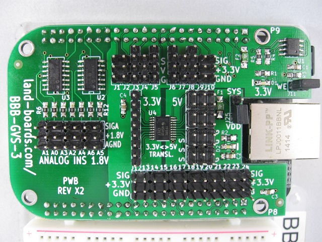
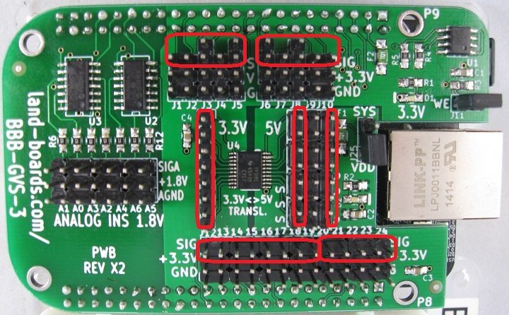
- (19) GPIOs, GVS pins
- GVS pins
- (3) UARTs, GVTxRx pins
- Gnd, Vcc, Tx, Rx pins
- (1) I2C bus, G, V, SDA, SCL
- Ground, Voltage, SDA, SCL
- (8) Channels of 3.3V to 5V level translators
- Use female to female jumpers to route the GPIO lines to the translator channels
- 5V side has GVS pins
- (7) 1.8V analog GVS connections with analog voltage/ground
- Buffer Opamps on the analog inputs
- 5V pins are all ESD protected pins with 15 kV of protection
- Selectable 5V source (SYS_5V or VDD_5V)
- LEDs for 3.3V and 5V power
- Cape configuration EEPROM with write enable jumper
- Beaglebone Black form factor
Connectors
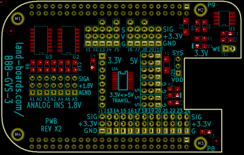
P8, P9 Connectors
Conn	GPIO		BBB Pin
J1	SPI1_D1		P9_30
J2	GPIO3_19	P9_27
J3_3	UART1_RX	P9_26
J3_4	UART1_TX	P9_24
J4	GPIO1_17	P9_23
J5_3	UART2_TX	P9_21
J5_4	UART2_RX	P9_22
J6_3	I2C1_SDA	P9_18
J6_4	I2C1_SCL	P9_17
J7	GPIO1_16	P9_15
J8_3	UART4_TX	P9_13
J8_4	UART4_RX	P9_11
J9	EHRPWM1A	P9_14
J10	GPIO1_28	P9_12
J12	GPIO1_29	P8_26
J13	EHRPWM2A	P8_19
J14	GPIO2_1		P8_18
J15	GPIO0_27	P8_17
J16	GPIO1_14	P8_16
J17	GPIO1_15	P8_15
J18	EHRPWM2B	P8_13
J19	GPIO1_12	P8_12
J20	GPIO1_13	P8_11
J21	TIMER5		P8_09
J22	TIMER6		P8_10
J23	TIMER4		P8_07
J24	TIMER7		P8_08
J11 - Write Enable (WE)
- Install for write enable
- Remove for write protect
EEPROM Connections
- The EEPROM connections are on I2C and have on-board pullup resistors.
- The connections are local to the card.
- The EEPROM part number is CAT24C256WI-GT3
Python pin assignments by header J number
J1 = "P9_30"		# GR-1 - D0
J2 = "P9_27"		# BL-1 - D16
J3_3 = "P9_26"		# VI-1 - D1
J3_4 = "P9_24"		# GY-1 - D17
J4 = "P9_23"		# WH-1 - D2
J5_3 = "P9_21"		# BL-1 - D18
J5_4 = "P9_22"		# BR-2 - D3
J7 = "P9_15"		# RD-2 - D19
J8_3 = "P9_13"		# OR-2 - D4
J8_4 = "P9_11"		# YL-2 - D20
J9 = "P9_14"		# GR-2 - D5
J10 = "P9_12"		# BU-2 - D21
J20 = "P8_11"		# VI-2 - D6
J21 = "P8_9"		# GY-2 - D22
J22 = "P8_10"		# WH-2 - D7
J23 = "P8_7"		# BL-2 - D23
J24 = "P8_8"		# BR-3 - D8
J12 = "P8_26"		# RD-3 - D24
J13 = "P8_19"		# OR-3 - D9
J14 = "P8_18"		# YL-3 - D25
J15 = "P8_17"		# GR-3 - D10
J16 = "P8_16"		# BU-3 - D26
J17 = "P8_15"		# VI-3 - D11
J18 = "P8_13"		# GY-3 - D27
J19 = "P8_12"		# WH-3 - D12
Production Testing
Setup
- Install BBB-GVS-3 on Rev C BeagleBone Black card
- Install shunt at SYS on J25 (5VSEL)
- Install shunt at WE
- Ethernet connection to BBB
- Power via 5V jack to BBB
- Verify 5V and 3.3V LEDs are lit
- BBB are located on the Secondary net at:
- BBB Rev C - 192.168.2.109
- BBB Rev B - 192.168.2.110
- Log in via putty
- User = root
- Password = enter
I2C Testing/EEPROM Programming
- Go to directory
- Program the EEPROM
- Verify by typing
cd ~/pyBBB/BBB-GVS-3/mkeeprom
cat data.eeprom > /sys/bus/i2c/devices/1-0054/eeprom
cat /sys/bus/i2c/devices/1-0054/eeprom | hexdump -C
- Result should be like -
00000000  aa 55 33 ee 41 30 42 42  42 2d 47 56 53 2d 33 00  |.U3.A0BBB-GVS-3.|
00000010  00 00 00 00 00 00 00 00  00 00 00 00 00 00 00 00  |................|
00000020  00 00 00 00 00 00 58 31  00 00 4c 61 6e 64 20 42  |......X1..Land B|
00000030  6f 61 72 64 73 2c 20 4c  4c 43 42 42 42 2d 47 56  |oards, LLCBBB-GV|
00000040  53 2d 33 00 00 00 00 00  00 00 00 00 30 30 30 30  |S-3.........0000|
00000050  00 00 00 00 00 00 00 00  00 00 00 00 00 00 00 00  |................|
*
000000e0  00 00 00 00 00 00 00 00  00 00 00 00 00 fa 01 f4  |................|
000000f0  00 fa 00 00 ff ff ff ff  ff ff ff ff ff ff ff ff  |................|
00000100  ff ff ff ff ff ff ff ff  ff ff ff ff ff ff ff ff  |................|
*
00008000
- Remove WE jumper
- Type
cat data.eeprom > /sys/bus/i2c/devices/1-0054/eeprom
- Result should be error
root@BBB01:~/pyBBB/BBB-GVS-3/mkeeprom# cat data.eeprom > /sys/bus/i2c/devices/1-0054/eeprom
cat: write error: Connection timed out
Analog Testing
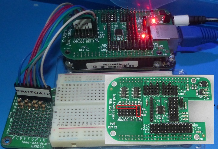
- Connect GRID49 card with resistor ladder
- (8) 10K resistors
- From 1.8V to all 7 inputs to ground
- Input in 1/8 steps
- Run analog ladder code
- PROTOA12 label plugs into resistor card with label facing towards resistors
- Green wire at A1 grid location on GRID49 card
- 3-pin connector goes to A5
- Label faces Ethernet jack
- Green wire goes to ground, white wire goes to +1.8V
- May need to run 2x to get accurate value
cd ~/pyBBB/BBB-GVS-3/analogLadder
python analogLadder.py
- Pass/Fail message will be displayed
val0  0.625
val1  0.125
val2  0.75
val3  0.24
val4  0.50
val5  0.375
val6  0.875
PASS - Analog values match expected ladder values
GPIO Testing
Cable set
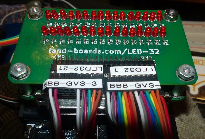
- Cables connect LED-32 card in ODAS Test Station to UUT
LED-32 connections
- Hook up LED-32 Card to these pins
BBB-GVS-3 connections
- Connect "loose" 1x8 cable marked "3.3V-SIG" from UUT 3.3V side of translator, connect to "J12-SIG" UUT J12
- Connect 1x8 cable from LED-32 marked "GND" to UUT 5V side of translator GND pins
- Connect 1x8 cable from LED-32 marked "5V-SIG" to UUT 5V side of translator
- Connect 1x5 cable from LED-32 marked "J20-SIG" to UUT J20 SIG pins
- Connect 2x5 cable from LED-32 marked "J1-SIG" to UUT J1
- Connect 2x5 cable from LED-32 marked "J7-SIG" to UUT J6
D0 = "P9_30"		# GR-1 - D0
D1 = "P9_26"		# VI-1 - D1
D2 = "P9_23"		# WH-1 - D2
D3 = "P9_22"		# BR-2 - D3
D4 = "P9_13"		# OR-2 - D4
D5 = "P9_14"		# GR-2 - D5
D6 = "P8_11"		# RD-3 - D6
D7 = "P8_10"		# YL-3 - D7
D8 = "P8_8"		# BU-3 - D8
D9 = "P8_19"		# GY-3 - D9
D10 = "P8_17"		# VI-2 - D10
D11 = "P8_15"		# WH-2 - D11
D12 = "P8_12"		# BR-3 - D12
D27 = "P8_13"		# BL-2 - D27
D26 = "P8_16"		# GY-2 - D26
D25 = "P8_18"		# WH-3 - D25
D24 = "P8_26"		# VI-3 - D24
D23 = "P8_7"		# GR-3 - D23
D22 = "P8_9"		# OR-3 - D22
D21 = "P9_12"		# BU-2 - D21
D20 = "P9_11"		# YL-2 - D20
D19 = "P9_15"		# RD-2 - D19
D18 = "P9_21"		# BL-1 - D18
D17 = "P9_24"		# GY-1 - D17
D16 = "P9_27"		# BL-1 - D16
# Common Ground
Run test
cd ~/pyBBB/BBB-GVS-3/blink-BBB-GVS-3/src
python blink-BBB-GVS-3.py
- Lights will circulate around the card in a ring
- CTRL-C to end test
Prepare to re-run
- Type
halt
- Remove 5V Power cable to power of card
Combined Copy/Paste
cd ~/pyBBB/BBB-GVS-3/mkeeprom
cat data.eeprom > /sys/bus/i2c/devices/1-0054/eeprom
cat /sys/bus/i2c/devices/1-0054/eeprom | hexdump -C

cd ~/BBB/BBB-GVS-3/analogLadder
python analogLadder.py

cd ~/pyBBB/BBB-GVS-3/blink-BBB-GVS-3/src
python blink-BBB-GVS-3.py

halt
Issues with X2 card
- No known or reported issues
Issues with X1 card
- WP jumper should be WE
- EEPROM A3 s/b high not low
- Cut etch to U1-3
- Add wire U1-3 to U1-8

