Difference between revisions of "SWLEDX8-I2C"
Jump to navigation
Jump to search
Blwikiadmin (talk | contribs) |
Blwikiadmin (talk | contribs) |
||
| Line 49: | Line 49: | ||
[[file:SWLEDX8-I2C_P1A.PNG]] | [[file:SWLEDX8-I2C_P1A.PNG]] | ||
| − | * MCP23017 Port A connects to SWITCHES 0-7 on [[SWLEDX8]] | + | ==== Connections to SWLEDX8 Card ==== |
| − | * MCP23017 Port B connects to LEDs 0-7 on [[SWLEDX8]] | + | |
| + | * When paired with SWLEDX8 | ||
| + | ** MCP23017 Port A connects to SWITCHES 0-7 on [[SWLEDX8]] | ||
| + | ** MCP23017 Port B connects to LEDs 0-7 on [[SWLEDX8]] | ||
[[file:SWLEDX8-I2C_P1.PNG]] | [[file:SWLEDX8-I2C_P1.PNG]] | ||
Revision as of 12:26, 24 May 2022
Contents
Features
- 16-Bit MCP23017
- I2C interface
- I2C Daisy-Chain (In/Out) connectors
- (3) I2C Address select jumpers for up to 8 devices per I2C bus
- SCL/SDA termination jumpers
- 2x10 pins
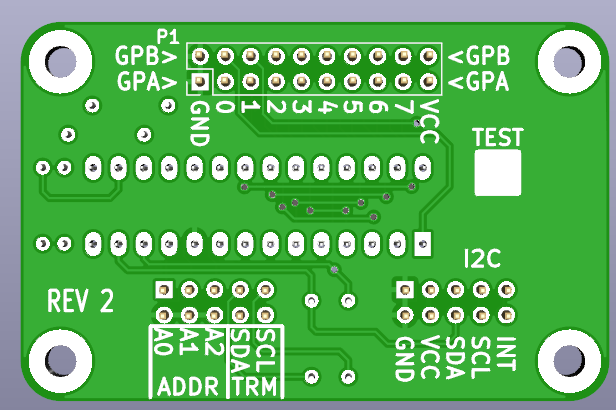
- 59mmx38mm
- (4) #4-40 mounting holes
- SWLEDx8-I2C can be used standalone or stacked together with the SWLEDX8 card
Build Options
- There are a number of options for using the card
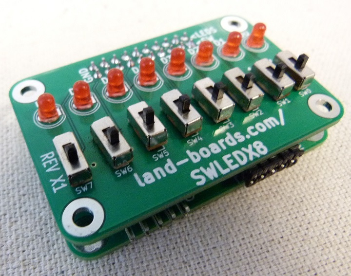
- Stacked option with SWLEDX8 card
- Small footprint
- Low height/profile
Stacked option with SWLEDX8 card
- SWLEDX8 card mounts above this card
- Pins can be directly mounted to both cards or male/female connector pairs can be used
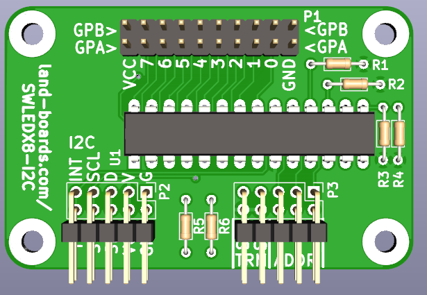
Small footprint option
Low height/profile option
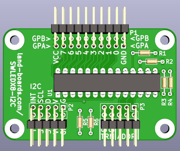
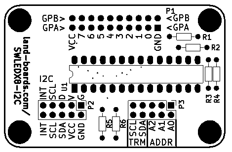
Rear Side Marking
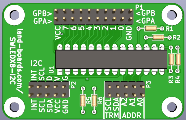
Connectors
- Connectors are as follows
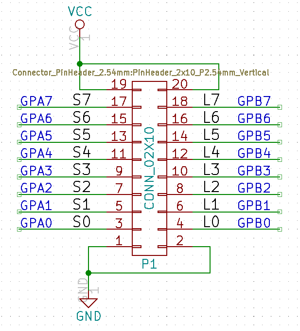
P1 - GPIO Pins
Connections to SWLEDX8 Card
- When paired with SWLEDX8
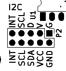
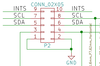
P2 - I2C Interface
- 2X5 header
- Pinout
- GND
- VCC
- SDA
- SCL
- INTA
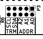
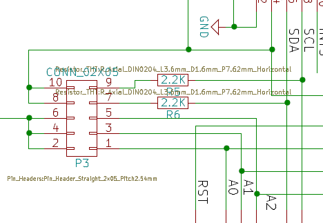
P3 - I2C Terminators / I2C Address Offset Jumpers
- Install left 2 jumpers to terminate I2C bus
- Typically, the "last" card in a chain
- Install right 3 jumpers for I2C base address offset in range 0x20 (all installed) to 0x27 (all removed)
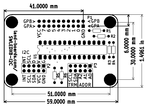
Mechanicals
Versions
Rev 2
- Functionally the same as Rev X1
- Change resistors from SMT (0805) to through hole (1/8W)
- Adds silkscreen Front/Rear
- Added test block to rear
Rev X1
- Words, no issues
