Difference between revisions of "UNI-OPAMP-04"
Jump to navigation
Jump to search
Blwikiadmin (talk | contribs) |
Blwikiadmin (talk | contribs) |
||
| Line 20: | Line 20: | ||
* 59X49mm form factor | * 59X49mm form factor | ||
* (4) 4-40 mounting holes | * (4) 4-40 mounting holes | ||
| + | |||
| + | === Typical OpAmps=== | ||
| + | |||
| + | {| class="wikitable" | ||
| + | ! Part | ||
| + | ! LM324 | ||
| + | ! MCP6004 | ||
| + | ! NJM2060 | ||
| + | |- | ||
| + | | Operating Voltage | ||
| + | | 3 to 30V | ||
| + | | 1.8V to 6V | ||
| + | | +/-4 to +/-18V | ||
| + | |- | ||
| + | | GBW Product | ||
| + | | 1.2 MHz | ||
| + | | 1 MHz | ||
| + | | 10 MHz | ||
| + | |- | ||
| + | | Output Current (mA) | ||
| + | | 10mA | ||
| + | | 23mA | ||
| + | | 25mA | ||
| + | |- | ||
| + | | Offset Voltage | ||
| + | | 7mV | ||
| + | | 4.5mV | ||
| + | | 6mV | ||
| + | |- | ||
| + | |} | ||
| + | |||
== Connectors == | == Connectors == | ||
Revision as of 15:02, 16 August 2022
Contents
Features
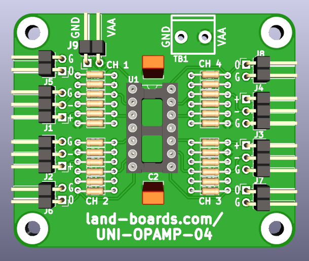
- Universal OpAmp Board
- Configurable through stuffing options for typical OpAmp circuits
- 4 Channels
- 1 Quad OpAmp
- Individual input and output headers per channel
- Terminal block or header for power
- Bypass capacitors
- 59X49mm form factor
- (4) 4-40 mounting holes
Typical OpAmps
| Part | LM324 | MCP6004 | NJM2060 |
|---|---|---|---|
| Operating Voltage | 3 to 30V | 1.8V to 6V | +/-4 to +/-18V |
| GBW Product | 1.2 MHz | 1 MHz | 10 MHz |
| Output Current (mA) | 10mA | 23mA | 25mA |
| Offset Voltage | 7mV | 4.5mV | 6mV |
Connectors
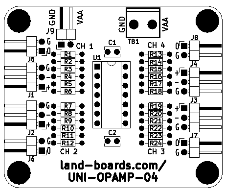
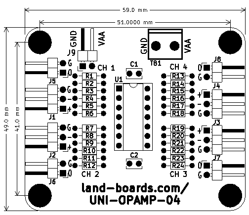
J1-J4 - Inputs
- Pinout
- Opamp + input
- Opamp - input
- GND
- J1 - CH 1
- J2 - CH 2
- J3 - CH 3
- J4 - CH 4
J5-J8 - Outputs
- Pinouts
- Opamp Out
- GND
- J5 - CH 1
- J6 - CH 2
- J7 - CH 3
- J8 - CH 4
Configurations
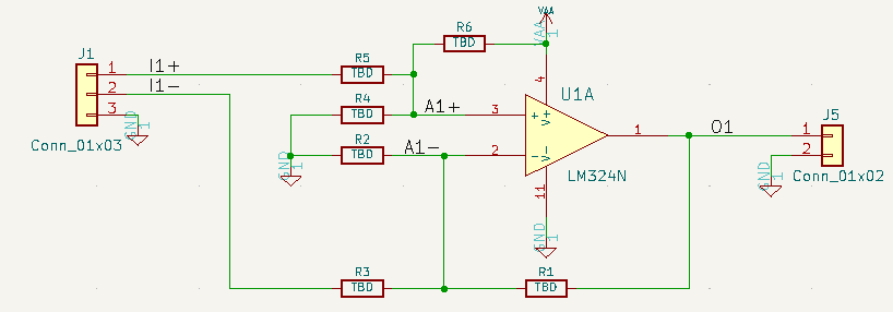
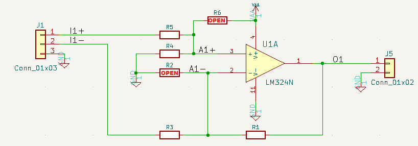
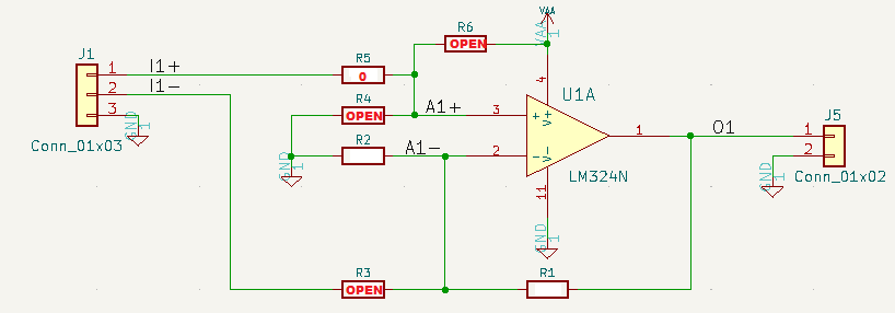
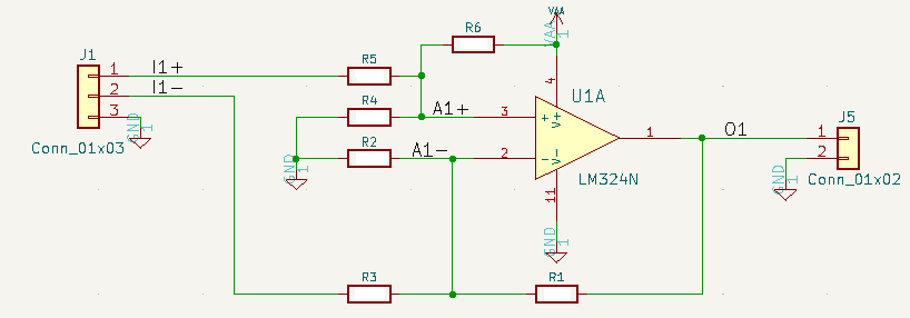
- The reference designs (below) are for the first channel.
- The resistor mapping from the first channel on the schematic to the other channels are as follows.
Resistor Stuffing by Channel
| OpAmp | Ax-/Ix- | Ax+/Ix+ | Ax-/Qx | Ax-/GND | Ax+/GND | Ax+/VCC |
|---|---|---|---|---|---|---|
| U1A | R3 | R5 | R1 | R2 | R4 | R6 |
| U1B | R10 | R9 | R12 | R11 | R7 | R8 |
| U1C | R22 | R19 | R24 | R23 | R21 | R20 |
| U1D | R15 | R17 | R13 | R14 | R16 | R18 |
Reference Designs
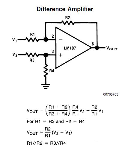
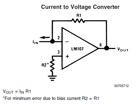
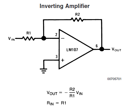
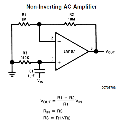
- Reference drawings are from TI Ap Note 31 - Op Amp Circuit Collection
- Reference designators are for channel 1
- See resistor values table (above) schematic for other channels

