Difference between revisions of "RF Noise Generator"
Jump to navigation
Jump to search
Blwikiadmin (talk | contribs) (→Design) |
Blwikiadmin (talk | contribs) |
||
| Line 18: | Line 18: | ||
* Unique nodes in red | * Unique nodes in red | ||
* Prototype on single sided copper clad PCB | * Prototype on single sided copper clad PCB | ||
| + | * KiCAD zener packages have backwards silkscreen (will need to fix on OshPark PCBs) | ||
[[file:NG-layout.PNG]] | [[file:NG-layout.PNG]] | ||
Revision as of 15:57, 21 August 2021
Contents
Design
- Useful as a filter test signal source
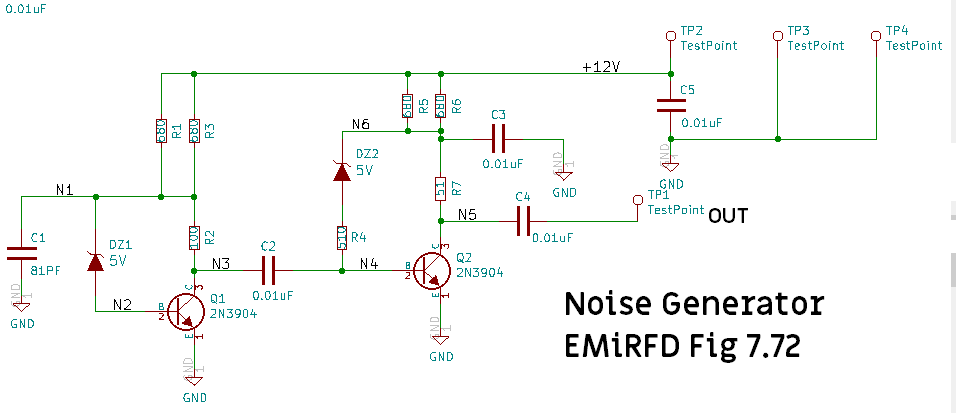
- From Experimental Methods in RF Design
- Fig 7.72
- Described as "not flat"
- "Junk box" parts
- (2) 2N3904 transistors
- (2) 5V (nominal) zener diodes
- Noise figure -50 dBm @ 10 MHz
Schematic
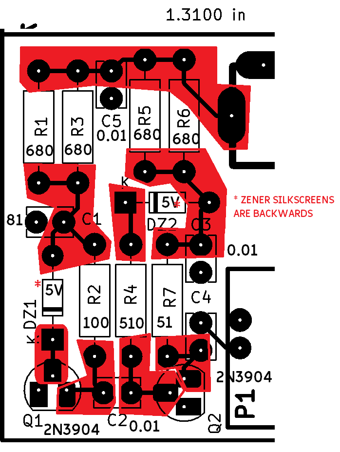
Prototype
- Unique nodes in red
- Prototype on single sided copper clad PCB
- KiCAD zener packages have backwards silkscreen (will need to fix on OshPark PCBs)

