Difference between revisions of "RF Noise Generator"
Jump to navigation
Jump to search
Blwikiadmin (talk | contribs) |
Blwikiadmin (talk | contribs) |
||
| Line 137: | Line 137: | ||
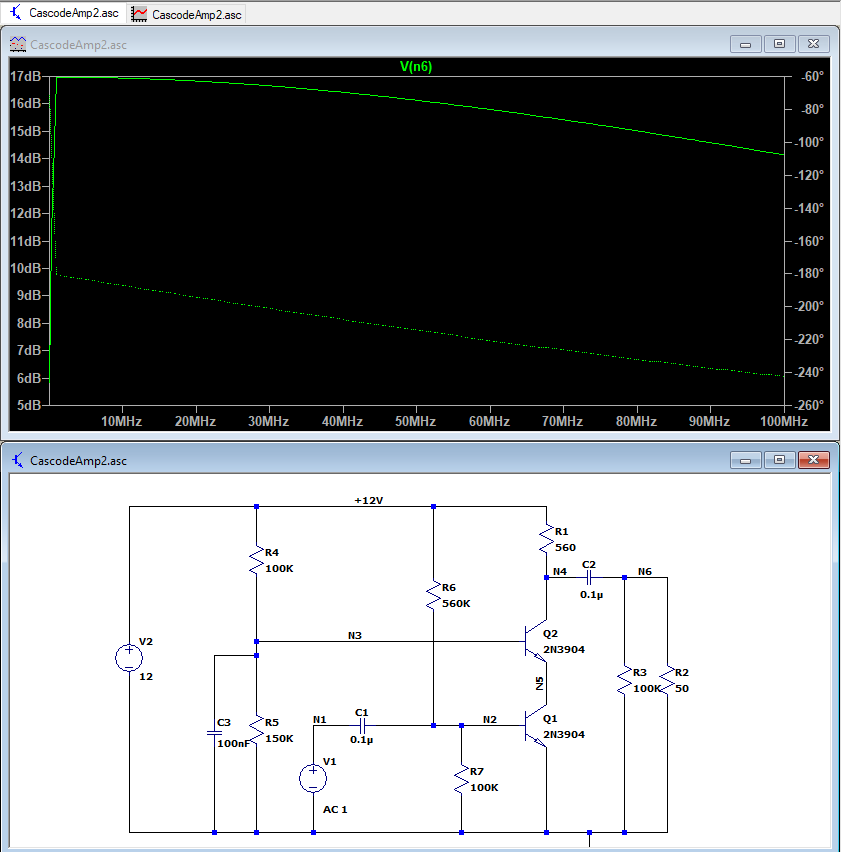
[[file:Cascode2_Sch.PNG]] | [[file:Cascode2_Sch.PNG]] | ||
| + | |||
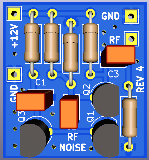
| + | [[FILE:NoiseGen_V3_3D.png]] | ||
* < 3 dB down at 100 MHz | * < 3 dB down at 100 MHz | ||
Revision as of 23:35, 1 October 2021
Contents
Design
- Useful as a filter test signal source
- Pass filters
- Crystal filters
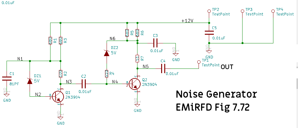
- From Experimental Methods in RF Design
- Fig 7.72
- Described as "not flat"
- "Junk box" parts
- (2) 2N3904 transistors
- (2) 5V (nominal) zener diodes
- Noise figure -50 dBm @ 10 MHz
Schematic
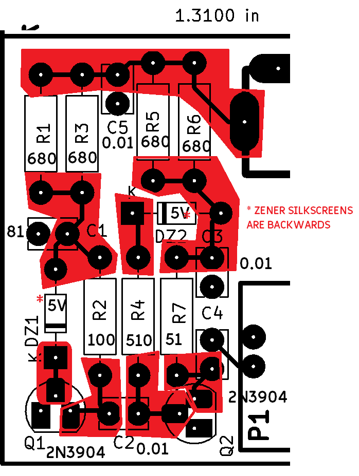
First Prototype
- Unique nodes in red
- Prototype on single sided copper clad PCB
- KiCAD zener packages have backwards silkscreen (will need to fix on OshPark PCBs)
Meaurements
- 12V, 43mA current draw
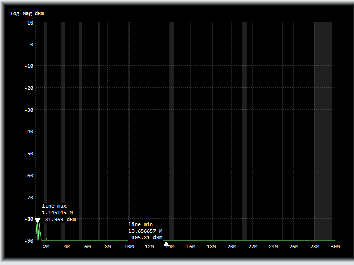
tinySA Measurements
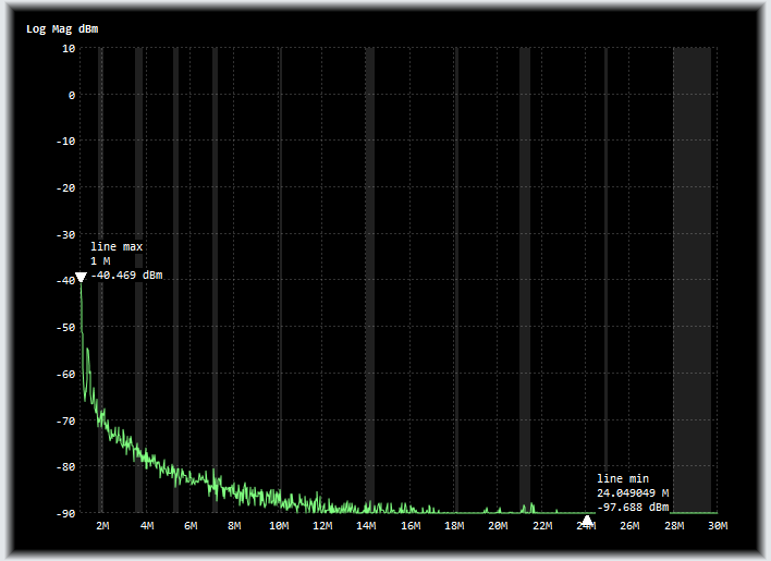
- 1-30 MHz
- Power Off
- Power On
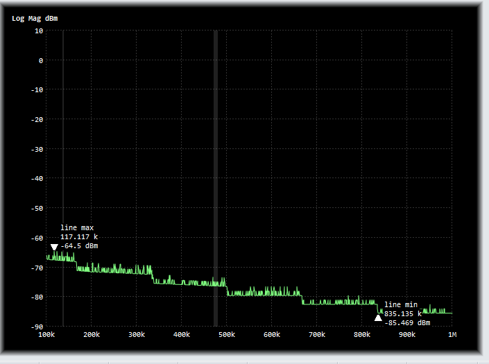
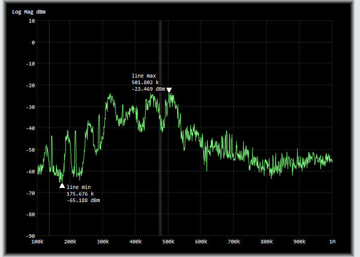
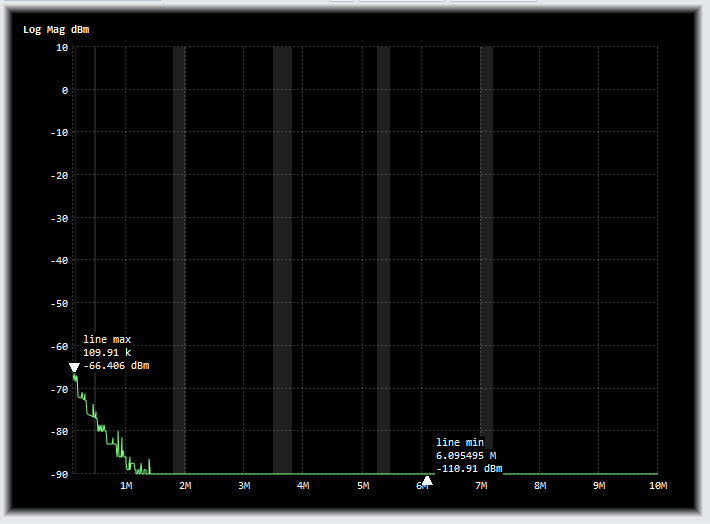
- 100 KHz-1 MHz
- Power Off
- Power On
- Lot more energy at ~400 KHz
- -30 dB
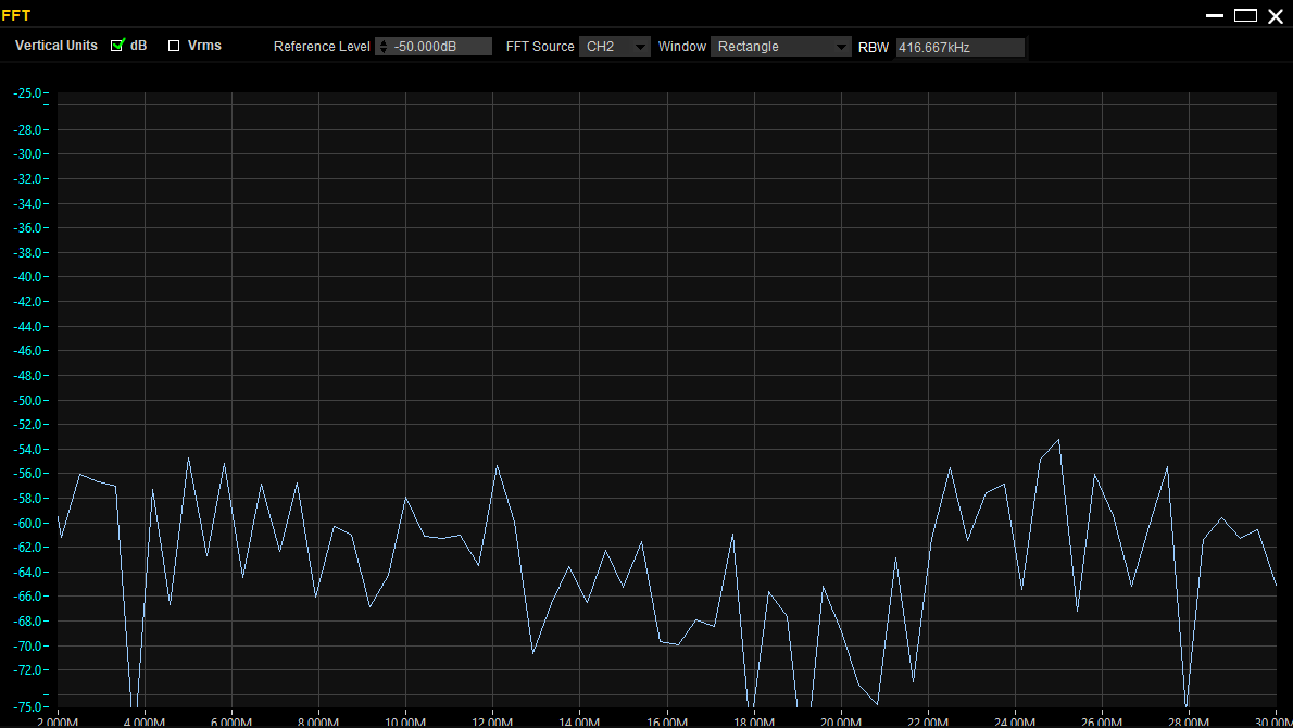
Rigol DS1054Z Measurements
- 50 MHz scope with mods
- UltraScope settings
- SCAL 1.00 V
- H 200nS
- FFT settings
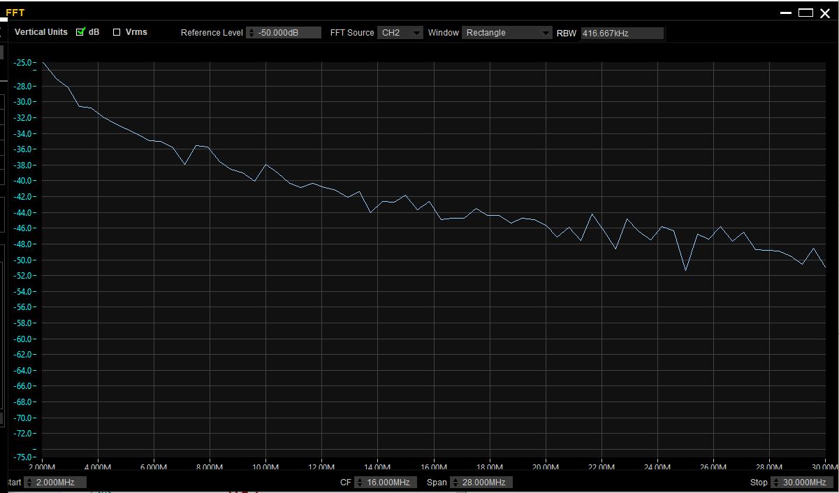
- CF = 16 MHz
- 2 MHz start, 50 MHz stop
- RBW 416.6 KHz
- Background noise
- Generator off
- Average ~ -64 dB
- Noise Generator On
- Falls off with frequency, but better than -50 dB
- Measured performance per EMiRFD (predicted - 50 dB)
Better Design #2
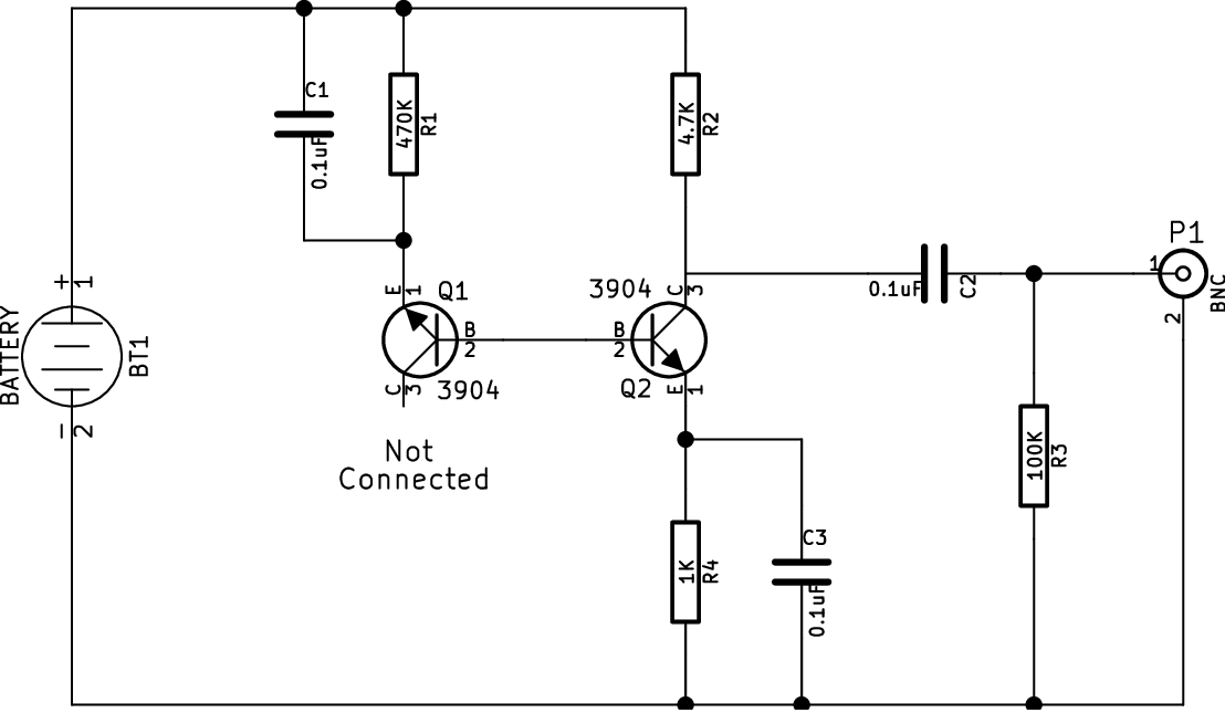
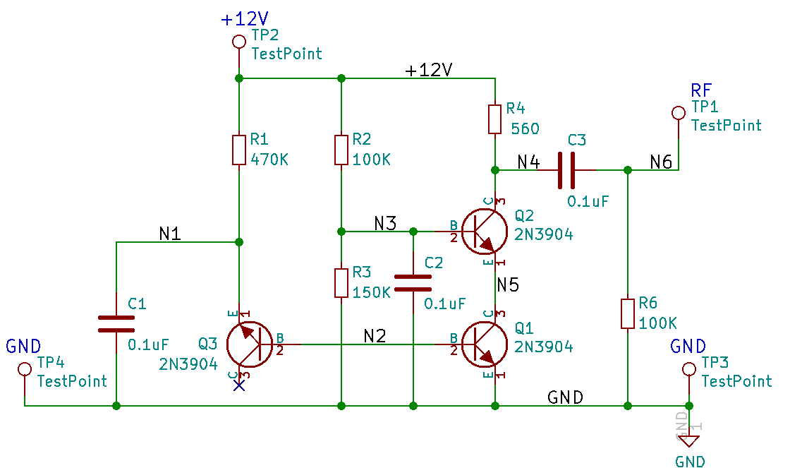
- Replace Zener as noise source with 2N3904 B-E junction reverse biased
- C1 is connected Emitter of Q1 to GND instead of +12V to reduce power supply noise
- Higher noise than EMiRFD design
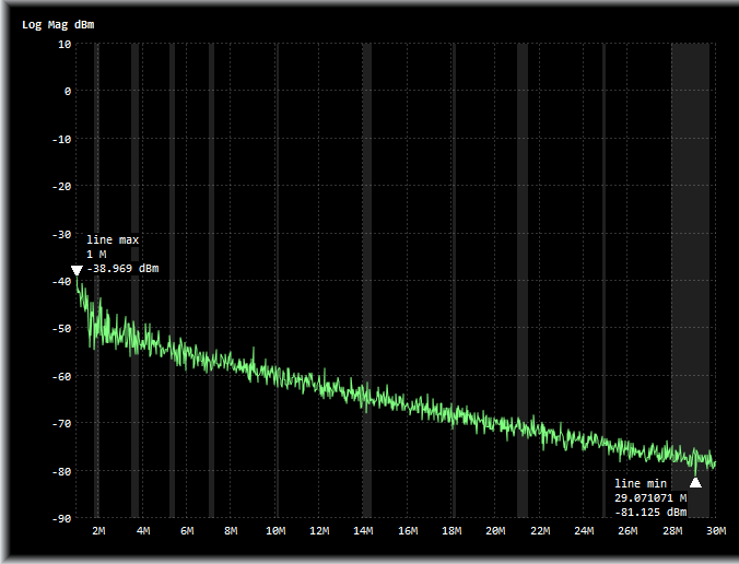
- Usable from 1-10 MHz
- -40 dBm at 1 MHz
- -80 dBm at 30 MHz
- Nearly zero power supply current
Better Design #2 - LTSPice Simulation
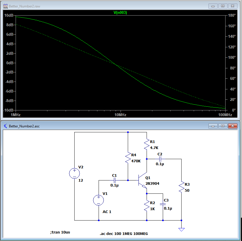
- Falls off in a straight line (in dBm) with frequency
- 10 dB at 1 MHz
- 0 dB at 10 MHz
- -10dB at 100 MHz
tinySA Measurements
- Off
- On, 1-30 MHz
- Consistent with the LTSpice simulation
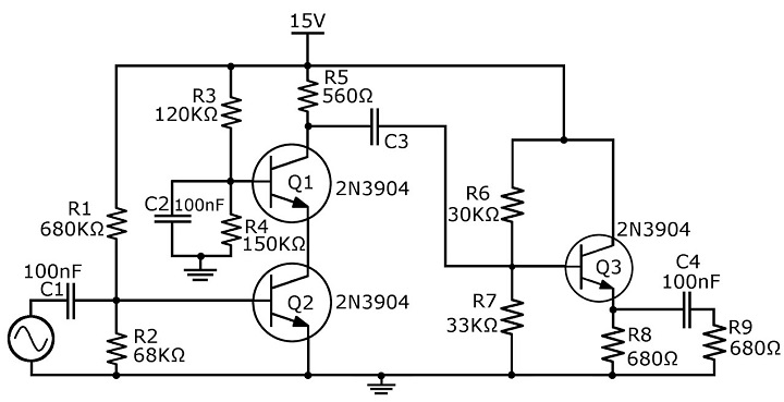
Better Design #3 - Cascode Amp with output buffer
- Previous design is probably good into receiver but not as good for tinySA tracking generator
- Want to be able to drive passive/crystal filters for testing
- Can already use NanoVNA but I'd prefer the tinySA due to lower noise floor
- Goal
- Flat response across 1-30 MHz
- Good parts of Design #2
- Transistor seems to be a better noise source than a zener
- Idea - replace amp stage with cascode output stage followed by emitter follower for better match to 50 ohm load
Example cascode design
- Replace R1 with 0.1uF in parallel with 470K (from the the previous)
- Remove R2
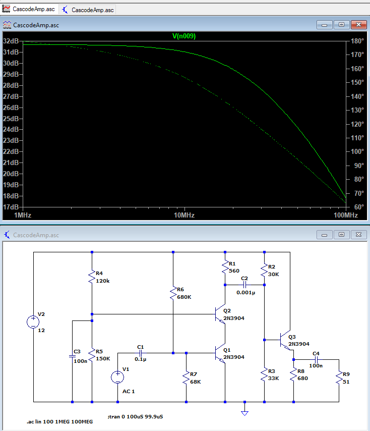
Better Design #3 - LTSpice Simulation
- Output stage is high gain, but limits bandwidth
Better Design #4
- #3 output stage was limiting
- Remove output stage
- < 3 dB down at 100 MHz
Cascode Videos
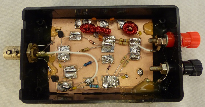
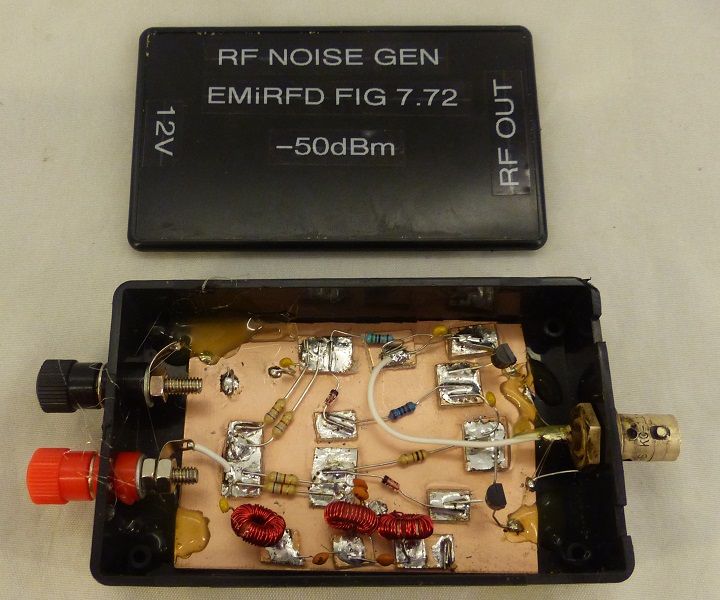
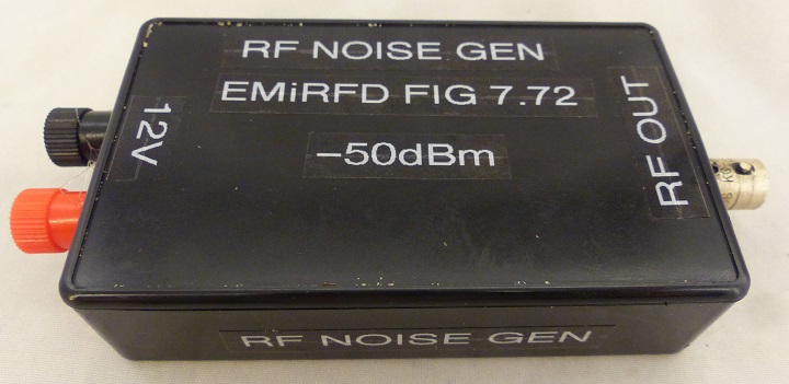
Build / Enclosure (Original board design)
- Used very old, but high quality chassis mount BNC connector
- Silver connector has a nice patina
- Built onto Single Side PCB material
- Acts as ground plane
- Pads cut from PCB material and superglued down onto the Base PCB
- Hot glued down into plastic enclosure
