MiniDuino
Contents
- 1 MiniDuino
- 2 Application-oriented Arduino variant
- 3 Embedded Design Arduino variant
- 4 Parametrics
- 5 Arduino Board Support Library
- 6 X2 Boards
- 7 Connectors/Pinouts
- 7.1 TB1 - 5mm Terminal block
- 7.2 J1 - TFT LCD
- 7.3 J2 - 5-Way Switch Menu (Analog 0)
- 7.4 J3 - GPS Connector (Digital 2/3)
- 7.5 J4 - FTDI (Digital 0/1)
- 7.6 J5 - Analog Spares (AD1-AD3) (Rev X2 board)
- 7.7 J6 - Digital Spares (D4-D6)
- 7.8 J7 - I2C Interface (AD4/AD5) (Rev X2 board)
- 7.9 J8 - Card Power Selection Jumper (FTDI or TB1)
- 8 Pins Assignments
- 9 Rev X1 Board
MiniDuino
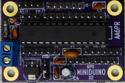
The MiniDuino is an Arduino(TM) variant targeted at a very specific application - an Embedded GPS controller. The functionality of the MiniDuino allows it to be used in many applications. MiniDuino is very small - 2.0" x 1.35" and has large 4-40 mounting holes on each of the four corners for easy installation into an enclosure.
Application-oriented Arduino variant
The MiniDuino is targetted at supporting some leading hardware choices. The following have connections directly on the MiniDuino:
- Adafruit Ultimate GPS Breakout 8-pin connector
- Chinese 1.8" TFT LCD with MicroSD Card (10 pin variant with wiring to support 8 pin wiring version) (Adafruit version).
- 6-pin connector
- 5-Way Switch interface (GVS)
- 5 Analog connections with AREF
- A4, A5 split onto separate I2C connector
- 3 Digital connections with Power/Ground
Embedded Design Arduino variant
The result is a great basis for most embedded designs. Any design which requires menu navigation and LCD displays along with a few I/O pins is a great fit. More I/O pins can be accommodated via an I2C interface and either the 8-bit I2C parallel port card or 16-bit I2C parallel port card.
MiniDuinoBlkDia.png
MiniDuinohookedup.JPG
Parametrics
Current draw 20 mA.
Arduino Board Support Library
Here's our Arduino library for the MiniDuino.
X2 Boards
MiniDuinoX2Front.JPG MiniDuinoX2Back.JPG
Take note of the header pin 1 orientations.
Connectors/Pinouts
Pin 1s are the square pins.
TB1 - 5mm Terminal block
The silkscreen for TB1 is marked with + and -.
Shunt Voltage Selected 1-2 VIN (7-12V) 2-3 GND Open Other (I/O pins)
J1 - TFT LCD
Pin Signal 1 VCC 2 BKLT (WIRED TO GROUND) 3 RESET 4 D/C-RES 5 MISO 6 MOSI 7 SCL 8 LCDCS 9 SDCS 10 GND
J2 - 5-Way Switch Menu (Analog 0)
GVS Connections
Pin Signal 1 GND 2 VCC 3 Switch Input
J3 - GPS Connector (Digital 2/3)
Pin Signal 1 VCC 2 GND 3 GPSRX 4 GPSTX 5 GPSFIX (N/C) 6 VBAT (N/C) 7 GPSEN (N/C) 8 3.3V OUT
J4 - FTDI (Digital 0/1)
Pin Signal 1 GND 2 GND 3 VCC 4 D0 5 D1 6 RESET
J5 - Analog Spares (AD1-AD3) (Rev X2 board)
Pin Signal 1 AREF 2 GND 3 GND 4 AD1 5 AD2 6 AD3
J6 - Digital Spares (D4-D6)
Pin Signal 1 VCC 2 D4 3 D5 4 D6 5 GND 6 GND
J7 - I2C Interface (AD4/AD5) (Rev X2 board)
Pin Signal 1 GND 2 VCC 3 SDA 4 SCL
J8 - Card Power Selection Jumper (FTDI or TB1)
Header	Function
1-2	FTDI
2-3	TB1
Open	Other connectors
Material costs
Ref	Value	Cost
C1	0.1uF	0.15
C2	0.1uF	0.15
C3	0.1uF	0.15
C4	CP	0.5
C5	0.1uF	0.15
D1	1N4004	0.3
J1	CONN_10	0.25
J2	CONN_3	0.15
J3	CONN_8	0.25
J4	CONN_6	0.25
J5	CONN_6	0.25
J6	CONN_6	0.25
J7	CONN_4	0.25
J8	CONN_3	0.25
MTG1	CONN_1	0
MTG2	CONN_1	0
MTG3	CONN_1	0
MTG4	CONN_1	0
R1	10K	0.1
TB1	TB-2PIN	0.5
U1	ATMEGA328-PU	3
U2	AP1117	0.5
Y1	16MHz	0.5
 	PCB	4.58
 	 Total	12.48
Pins Assignments
// Pin assignments as referenced to the Zachary ProtoShield // Arduino Port Connector Function // D0 J4-4 FTDI Transmit/Arduino Receive // D1 J4-5 FTDI Receive/Arduino Transmit // D2 J3-3 GPSRx // D3 J3-4 GPSTx // D4 J6-2 Digital Input // D5 J6-3 Digital Input // D6 J6-4 Digital Input // D7 J1-9 SD Card Chip Select // D8 J1-3 LCD Reset // D9 J1-4 LCD Register Select (DC or RS) // D10 J1-8 LCD Chip Select // D11 J1-6 LCD MOSI // D12 J1-5 LCD MISO // D13 J1-7 LCD SCK // A0 J2-3 Keypad // A1 J5-4 Values (such as temperature) set potentiometer wiper // A2 J5-5 Analog Input // A3 J5-6 Analog Input // A4 (SDA) J7-3 I2C SDA LCD // A5 (SCK) J7-4 I2C SCK LCD
Rev X1 Board
J5 - Analog Spares (AD1-AD5) (Rev X1 board)
Pin Signal 1 AREF 2 GND 3 GND 4 AD1 5 AD2 6 AD3 7 AD4 8 AD5
