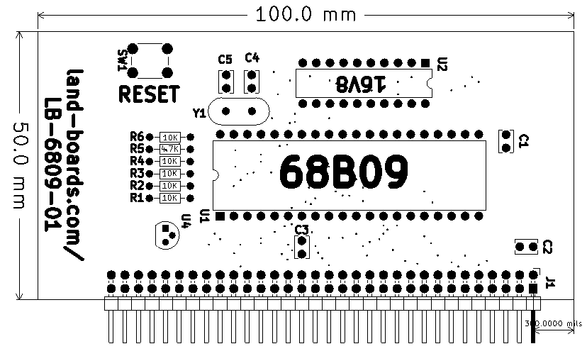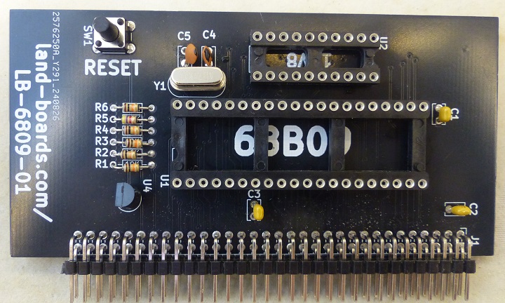
Features
- 68B09 CPU
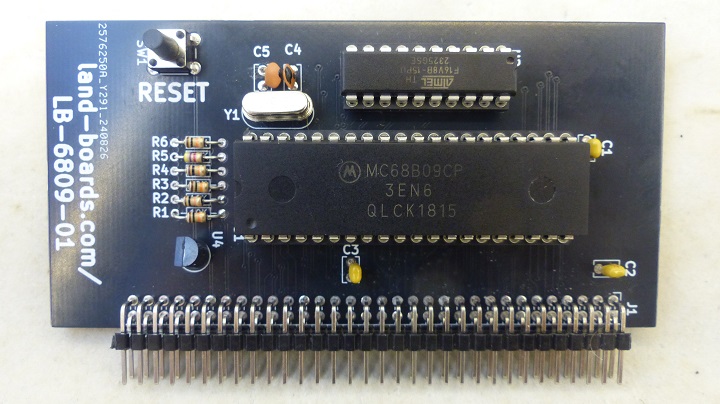
- 8 MHZ crystal on card
- Reset switch/power monitor
- Address decoder PLD drives RAM/ROM/IO chip selects
- 100x50mm card
Memory Map
- 0x0000-0x7FFF 32KB SRAM
- 0x8000-0x9FFF Free Space (8KB)
- 0xA000-0xBFFF Serial (ACIA)
- 0xC000-0xFFFF 16KB EPROM
Design
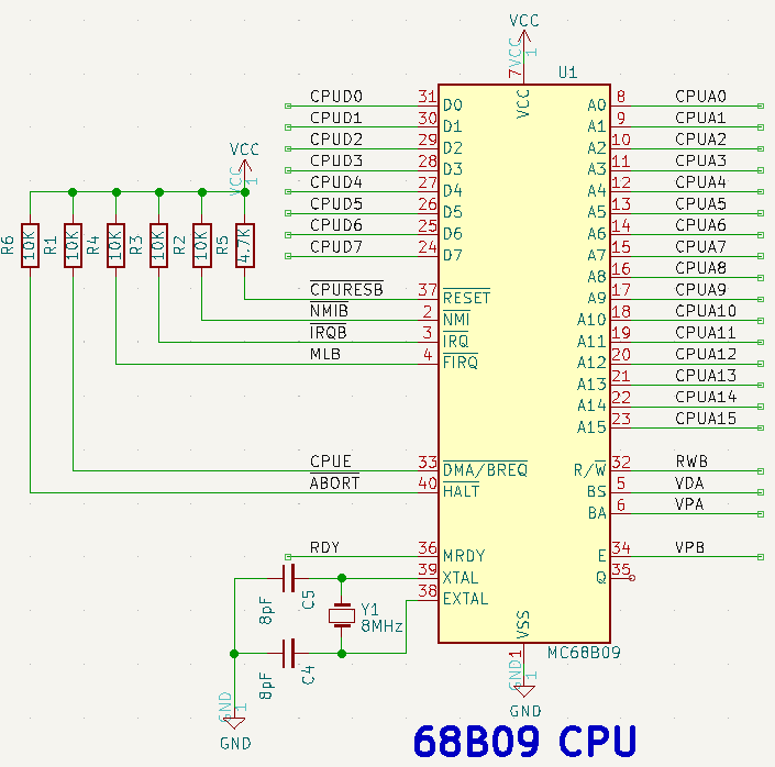
68B09 CPU
- 8 MHz clock
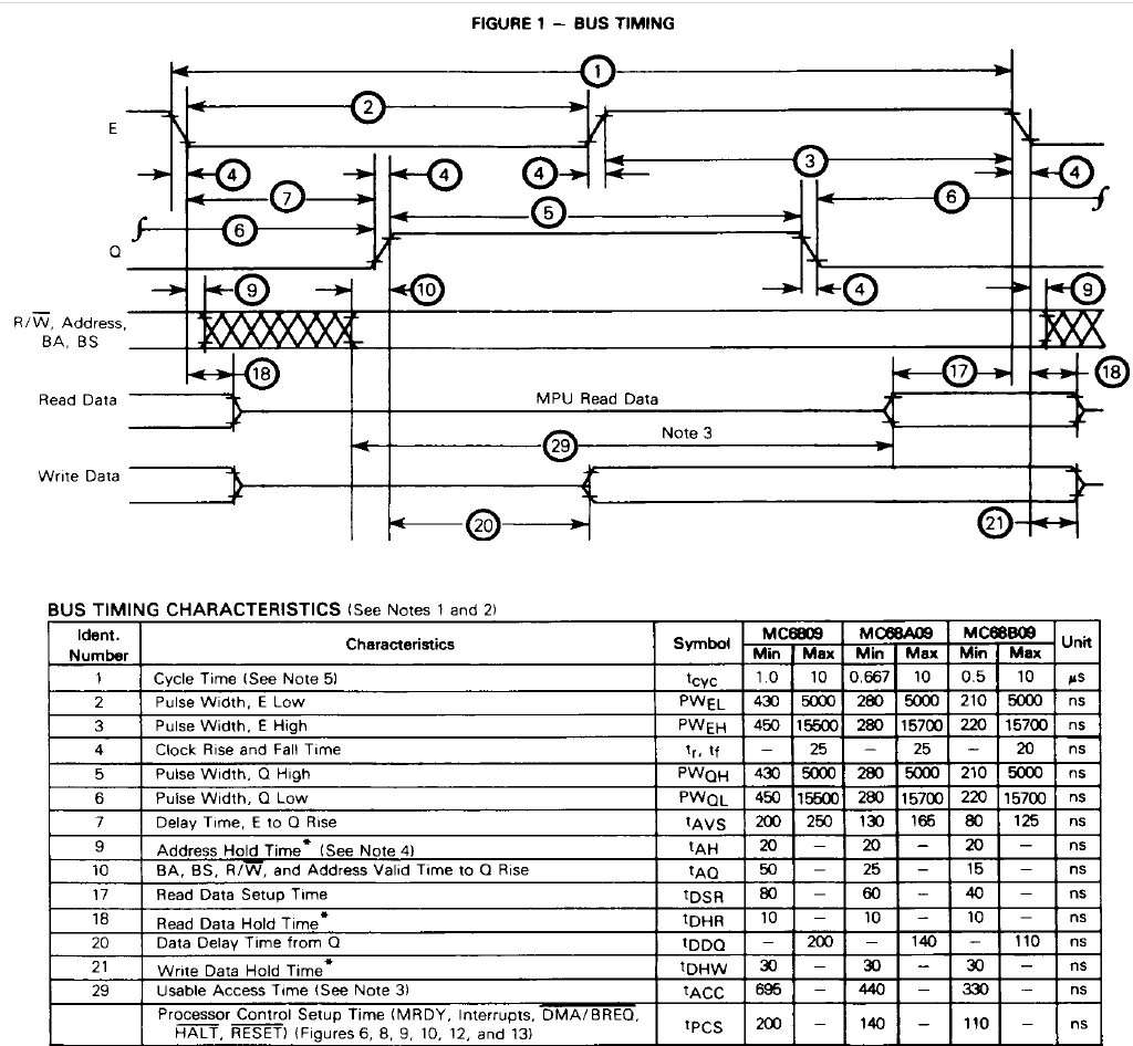
- Runs effectively at 2 MHz
CPU - Rev 2

CPU - Rev 1

CPU Timing

Clock
Crystal - Rev 2
- Uses CPU internal oscillator
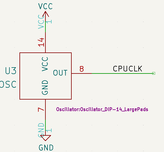
Oscillator - Rev 1
- 8 MHz oscillator for 2 MHz operation

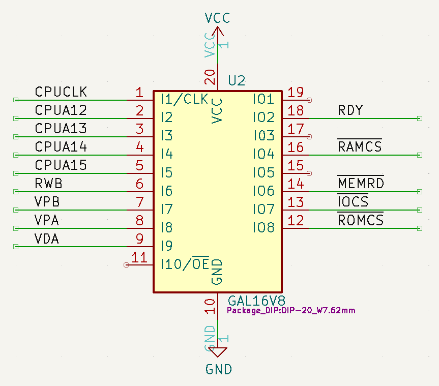
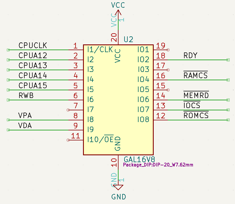
PLD
PLD on Card Rev 2

PLD on Card Rev 1

- Wire added (Rev 1) from E pin of CPU to PLD pin 7
PLD Listing
Name       LB-6809-01_PLD;
Partno     ATF16V8B;
Date       08/19/24;
Revision   01;
Designer   DOUG G;
Company    LAND BOARDS LLC;
Assembly   LB680901_U2;
Location   Rustbelt, US;
Device     G16V8;

/*
*/


/* Control inputs */
PIN    1   = CLK;
PIN    2   = CPUA12;
PIN    3   = CPUA13;
PIN    4   = CPUA14;
PIN    5   = CPUA15;
PIN    6   = CPUREAD;
PIN    7   = VPB;		/* Added as wire on Rev 1 PCB	*/
PIN    8   = VPA;
PIN    9   = VDA;

/* Address Decode and Chip Select outputs */
PIN    12  = !ROMCS;
PIN    13  = !IOCS;
PIN    14  = !MEMRD;
PIN    16  = !RAMCS;
PIN    18  = RDY;

ROMCS = CPUA15 & CPUA14 & VPB;

RAMCS = !CPUA15 & VPB
#        CPUA15 & !CPUA14 & !CPUA13 & VPB;

IOCS = CPUA15 & !CPUA14 & CPUA13 & VPB;

RDY = VPB;

MEMRD = CPUREAD & VPB;
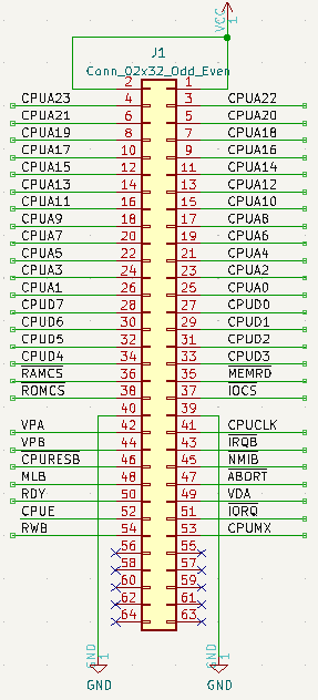
Backplane connector

Software
- LB-6809 code examples
- asm6809 - portable cross assembler targeting the Motorola 6809
- Features arbitrarily complex expressions (with most C-style operators available), forward references, macro expansion and conditional assembly
- Output formats are: Motorola SREC, Intel HEX (and others)
- asm6809 Manual
- Using asm6809 version 2.13
- asm6809-2.13-w64 Local copy
Build 6809 Assembly Code (Windows 64-bit)
- Run asm6809 in Windows CMD prompt window
[path_to_asm6809.exe_program\]asm6809 loop.asm -H -l -o loop.hex
- -H option creates hex record file to download to programmer
- -l fileName option creates listing file
- -o filename option followed by output file name
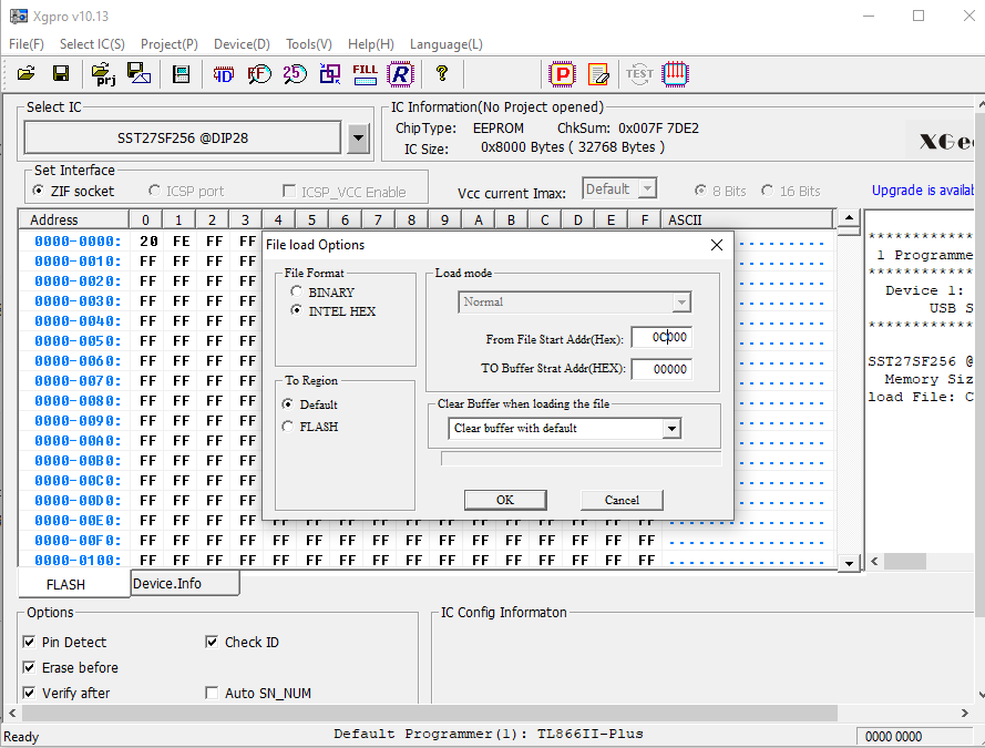
Programming using TL866

ROM access test code
..\..\M6809_Assembler\asm6809-2.13-w64\asm6809 loop.asm -H -l loop.lst -o loop.hex
		ORG $C000
RESVEC	BRA	RESVEC
		ORG	$FFFE
LBFFE	FDB	RESVEC	         ; RESET
:02C0000020FE20
:02FFFE00C00041
:00000001FF
Reference Designs
Mechanicals
Rev 2

Checkout
Rev 2 Checkout

Rev 2 PCB Changes from Rev 1
- Add U1-34 to U2-7 (VPB/E)
- Eliminate oscillator
- Add 8 MHz crystal/caps
- Cheaper and easier to find
- Add 4.7K pullup to U1-40 (ABORT*/HALT) line
- Change resistor values to lighten up Iol
- Beef up power plane connections to J1 and CPU/cap
- Move reset switch to the top of the board (where the oscillator used to be)


Rev 1 Checkout Notes
- Did not build
- Add wire U1-34 to U2-7 (VPB/E)
- Ground XTAL pin on CPU U1-39 (to U1-1 = GND)
- Use BOM for resistor values, not silkscreen
- Add 4.7K pullup to ABORT* line
Assembly Sheet
Rev 2
Rev 1
