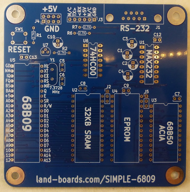
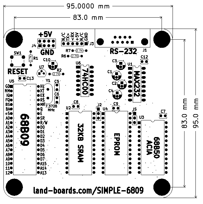
SIMPLE-6809
Revision as of 03:16, 11 September 2024 by Blwikiadmin (talk | contribs) (→ROM BASIC assembly listing)
Contents
Features
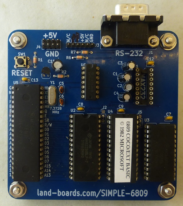
- Build of Grant Searles's Simple 6809 CPU
- Runs BASIC
- 68B09 CPU
- 7.3728 MHz
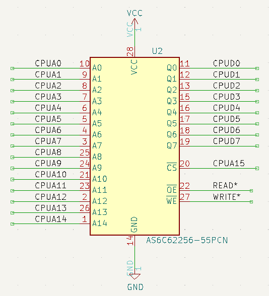
- 32KB SRAM
- 16KB EPROM/EEPROM
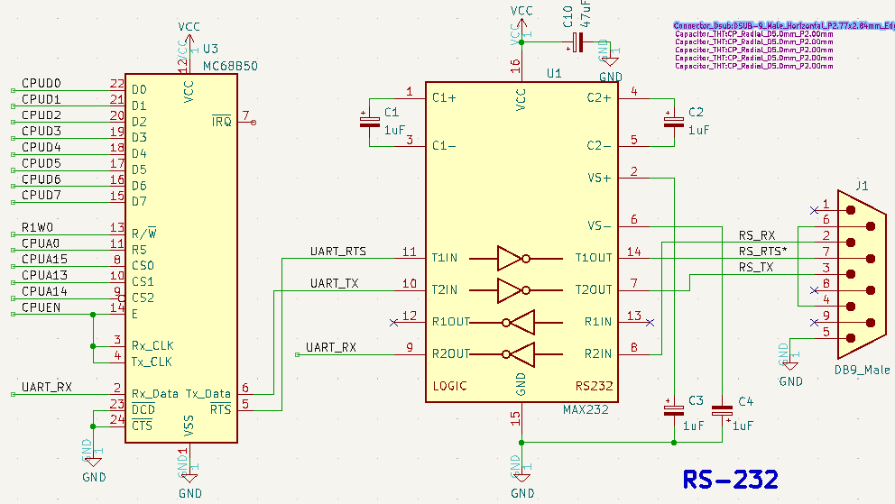
- 68B50 Serial Port (ACIA)
- RS-232 port
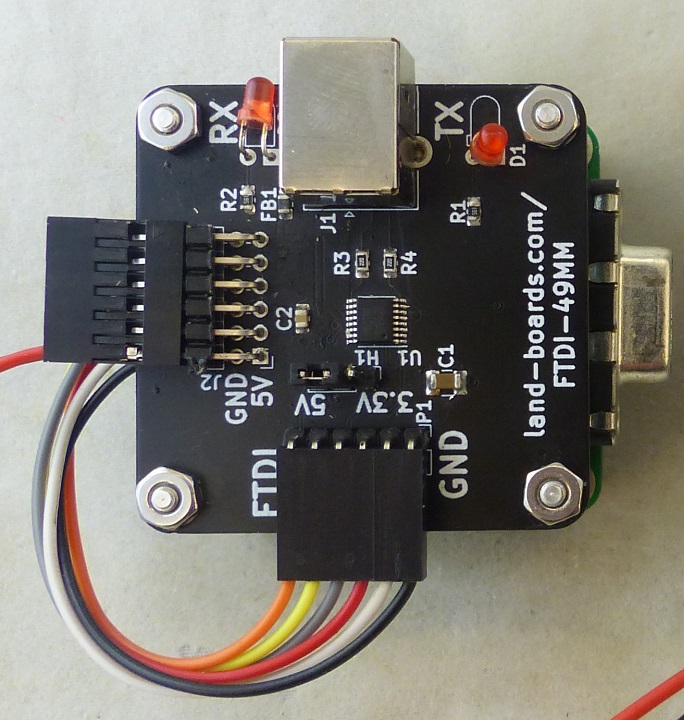
- Header for FTDI
- 115,200 baud
- Reset switch with optional Power Supervisor
- 95x95mm card
- (4) 6-32 mounting holes
Memory Map
- 0x0000-0x7FFF 32KB SRAM
- 0x8000-0x9FFF Free Space (8KB)
- 0xA000-0xBFFF Serial (ACIA)
- 0xC000-0xCFFF 16KB EPROM
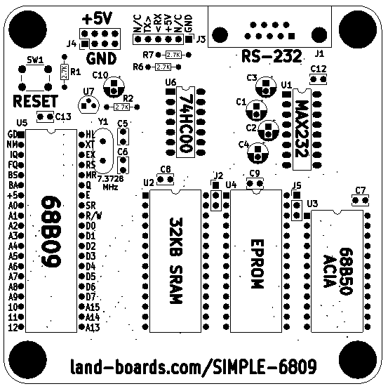
Chipset
Design
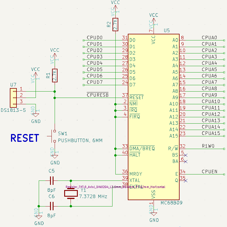
CPU
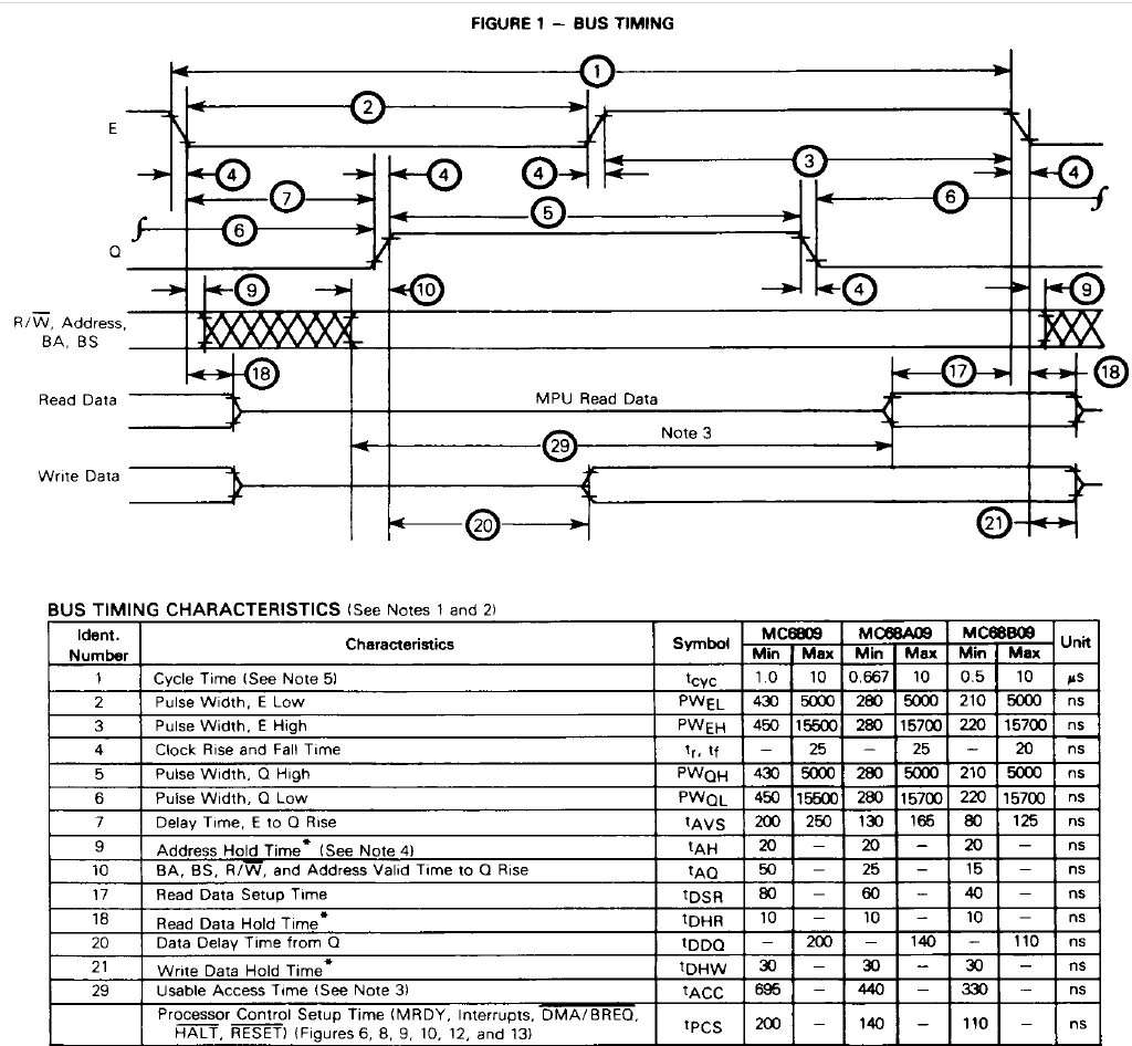
CPU Timing
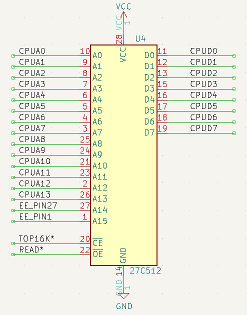
EEPROM
SRAM
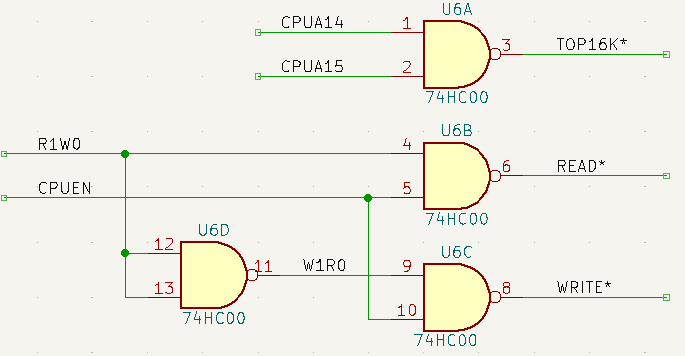
Logic
ACIA
- Can only use RS-232 or FTDI - one at a time
- Put MAX232 in a socket if you want flexibility
- Remove MAX232 if you want to use FTDI
Headers / Connectors
J1 - RS-232 Serial
- DB-9 Male
- Pinout
- N/C
- Receive
- Transmit
- Loop to pin 6
- GND
- Loop to pin 4
- RTS
- N/C
- N/C
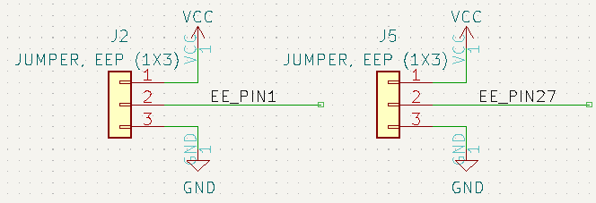
J2 / J5 - EPROM/EEPROM Select Jumpers
- J2 - EPROM Pin 1 jumper
- 1-2 for 28C64, 28C256 (Pull WE to VCC)
- 2-3 for 27256, 27SF256, 27512 (Pull A14 to GND)
- J5 - EPROM Pin 27 jumper
- GND (2-3)
EEPROM Pin Table
| 27512 | 27256 | 27SF256 | 28C256 | 27128 | 2764 | 28C64 | PIN | PIN | 2764 | 28C64 | 27128 | 28C256 | 27SF256 | 27256 | 27512 | |
|---|---|---|---|---|---|---|---|---|---|---|---|---|---|---|---|---|
| A15 | VPP | VPP | A14 | VPP | VPP | N/C | 1 | 28 | VCC | VCC | VCC | VCC | VCC | VCC | VCC | |
| A12 | A12 | A12 | A12 | A12 | A12 | A12 | 2 | 27 | PGM | WE* | PGM | WE* | A14 | A14 | A14 | |
| A7 | A7 | A7 | A7 | A7 | A7 | A7 | 3 | 26 | A13 | N/C | A13 | A13 | A13 | A13 | A13 | |
| A6 | A6 | A6 | A6 | A6 | A6 | A6 | 4 | 25 | A8 | A8 | A8 | A8 | A8 | A8 | A8 | |
| A5 | A5 | A5 | A5 | A5 | A5 | A5 | 5 | 24 | A9 | A9 | A9 | A9 | A9 | A9 | A9 | |
| A4 | A4 | A4 | A4 | A4 | A4 | A4 | 6 | 23 | A11 | A11 | A11 | A11 | A11 | A11 | A11 | |
| A3 | A3 | A3 | A3 | A3 | A3 | A3 | 7 | 22 | OE* | OE* | OE* | OE* | OE* | OE* | OE* | |
| A2 | A2 | A2 | A2 | A2 | A2 | A2 | 8 | 21 | A10 | A10 | A10 | A10 | A10 | A10 | A10 | |
| A1 | A1 | A1 | A1 | A1 | A1 | A1 | 9 | 20 | CE* | CE* | CE* | CE* | CE* | CE* | CE* | |
| A0 | A0 | A0 | A0 | A0 | A0 | A0 | 10 | 19 | D7 | D7 | D7 | D7 | D7 | D7 | D7 | |
| D0 | D0 | D0 | D0 | D0 | D0 | D0 | 11 | 18 | D6 | D6 | D6 | D6 | D6 | D6 | D6 | |
| D1 | D1 | D1 | D1 | D1 | D1 | D1 | 12 | 17 | D5 | D5 | D5 | D5 | D5 | D5 | D5 | |
| D2 | D2 | D2 | D2 | D2 | D2 | D2 | 13 | 16 | D4 | D4 | D4 | D4 | D4 | D4 | D4 | |
| GND | GND | GND | GND | GND | GND | GND | 14 | 15 | D3 | D3 | D3 | D3 | D3 | D3 | D3 |
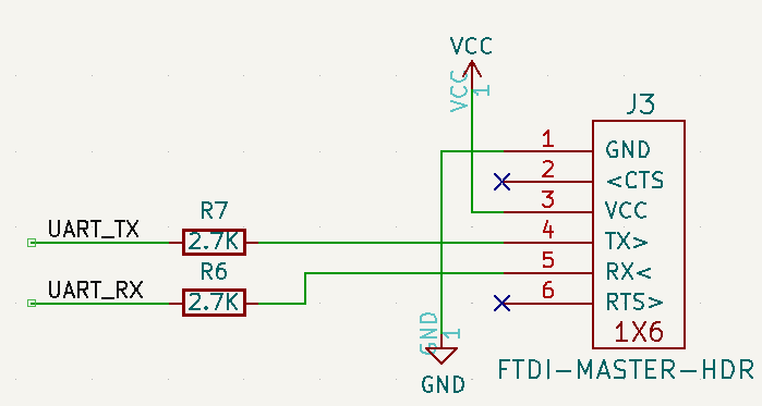
J3 - FTDI / TTL Serial
- Requires a FTDI cross-over cable
- Can only use RS-232 or FTDI - one at a time
- Put MAX232 in a socket if you want flexibility
- Remove MAX232 if you want to use FTDI
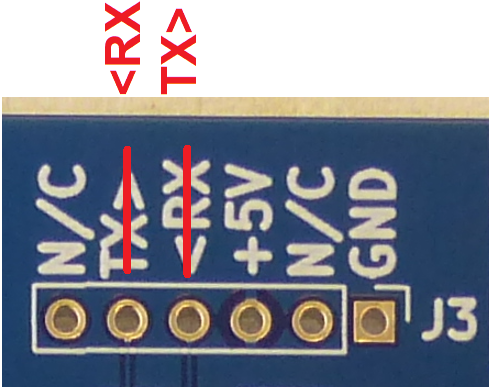
- Rev 1 PCB silkscreen is wrong (both sides of the card)
- GND
- N/C
- +5V
- Transmit (out)
- Receive (in)
- N/C
J4 - 5V Power
- 2x4 header
First Unit Checkout
Install Sockets
- Machined pin sockets
Install Passives
Power
- Install 2x4 at J4
- Power card via J4 with 5V
- Check power pins on parts
Clock
- Install Clock parts
- Install 7.3728 MHz crystal
- Install C5, C6
- Install CPU at U5
Reset
- Install U7 Power Monitor
- Install pushbutton switch SW1
- Reset button gets stretched by Power Monitor U9
- Measure reset at 68B09 U5 pin 37
- Falling edge scope cap
EPROM
- SST27C256 EEPROM
- 32 KB part
- Using first 16KB of EEPROM
- J2 EEPROM pin 1 = VPP = VCC or GND
- Jumper J2:2-3
- J5 EEPROM pin 27 = A14 = GND
- Jumper J5:2-3
- U1 - Do not install MAX232
- Use FTDI connector with FTDI-49MM card
EEPROM Programming
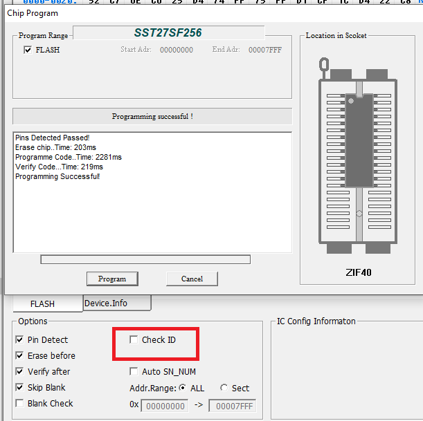
- Program using TL-866ii plus programmer
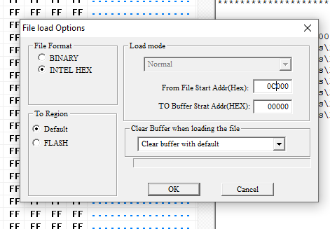
- File = ExBasROM.hex
- Set offsets for 27SF256 part
- Part is 32 KB
- hex files is 16 KB
- Set From File Start Addr(Hex) to 0C000
- To Buffer Start Addr(Hex) to 00000
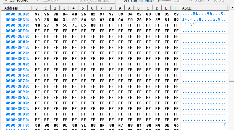
- Memory Buffer should look like
- Got Device ID error
- Turn off ID check
- Device programmed/verified
Install CPU, ROM, RAM, ACIA
- Do not install MAX232 yet
- Use FTDI connector with FTDI-49MM card
Test FTDI Serial
- Silkscreen swapped for TX, RX
Test RS-232 Serial
- With MAX232
- Install DB-9 Male
- Holes don't line up well, but 4-40 screws can fit
- Connected to FTDI-49MM and DCE cards
- Works
Software
- ExBasROM.hex - ROM file
ROM BASIC assembly listing
- AS9 was used to assemble the BASIC listing
- Grant wrote a serial handler to control the text I/O, along with suitable Control-C break handling
- Includes commands from the "Extended" BASIC ROM (from the "Extended BASIC Unraveled II" book)
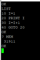
- The ROM in the SBC is fully working with all the commands in the Standard and Extended ROMS that are applicable to the SBC
- Assembled using as9 with the following command...
as9 exbasrom.asm -now l s19
- *-now" suppresses warnings
- "l" produces a lst file
- "s19" produces an s19 hex file
- If you use as9, you will probably get a "Null pointer assignment" message when it completes
- This can be ignored, and is a known bug with as9 that doesn't affect operation (according to the readme file that came with it)
- MBasROM.hex
- Hex file for 27C512
- Will need to be shifted down
- Hex file for 27C512
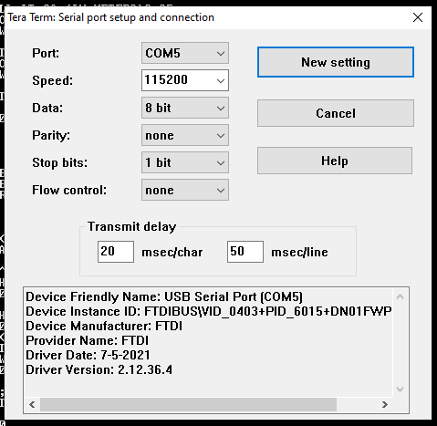
- 115,200 BAUD
- Same build as SIMPLE-6809 from Grant Searle
- Works
Performance
- TeraTerm settings
- Test software
10 FOR I =1 TO 10000
20 PRINT I
30 NEXT I
- Time ~52 secs
PCB Issues
Rev 2
- Fix Silkscreen on J3 (see above J3 FTDI cable section)
- Ordered 10 PCBs from JLCPCB
Rev 1
- Works
- Silkscreen J3 is wrong directions (TX/RX)

