Kits and Parts Mixers
Revision as of 12:03, 5 November 2021 by Blwikiadmin (talk | contribs) (→Kits and Parts Diode Mixer)
Contents
Kits and Parts Mixers - Features in Common
- Available as discrete diode or ADE-1 mixer cards from Kits and Parts
- LO, IF, RF Ports are all 50Ω
- +7dBm Local Oscillator injection level
- As measured into 50Ω load
- Mixers are not linear and loads should not be measured at the mixer
- As measured into 50Ω load
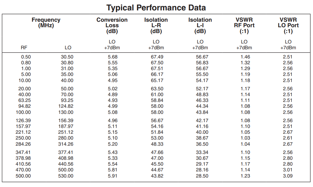
- ~5dB RF > IF conversion loss in HF region
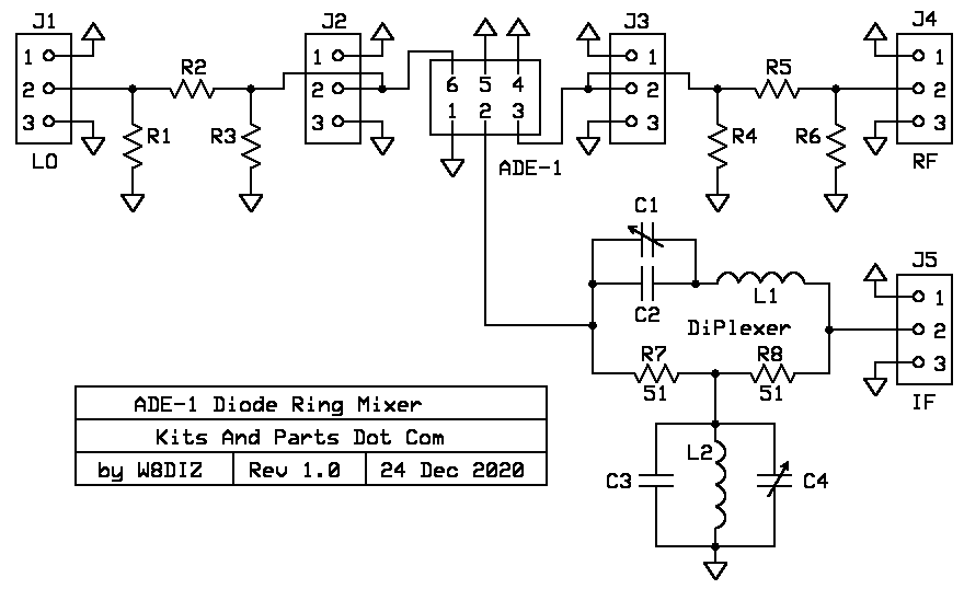
- Full Diplexer at the IF Port
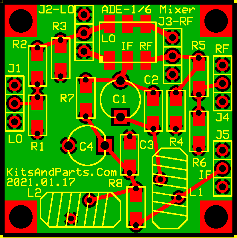
- Board has pads (SMT or 1/8W resistor pads) for optional Attenuators on RF & LO Ports
- 3 pin, 0.1" pads at board edges allow SMA edge connectors to be used
- Mounting holes in all 4 corners
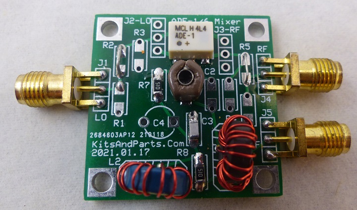
Kits and Parts ADE-1 Mixer
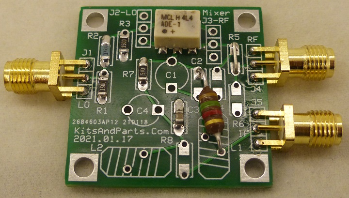
- Kits and Parts Mixer
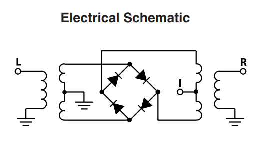
- Mini-Circuits ADE-1+ Double Balanced Diode Mixer with built in 50Ω transformers
- Not necessary to build and tune diplexer first if using NanoVNA and/or tinySA
- Only 1 cap adjust
- Inductors can also be spread/compressed if needed
- Available from Kits and Parts as bare PCB or kit of parts
- Bare board - $5
- Kit - $14
- Good deal since the mixer itself is $6
ADE-1 Schematic
Performance
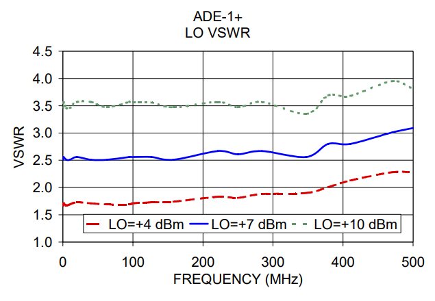
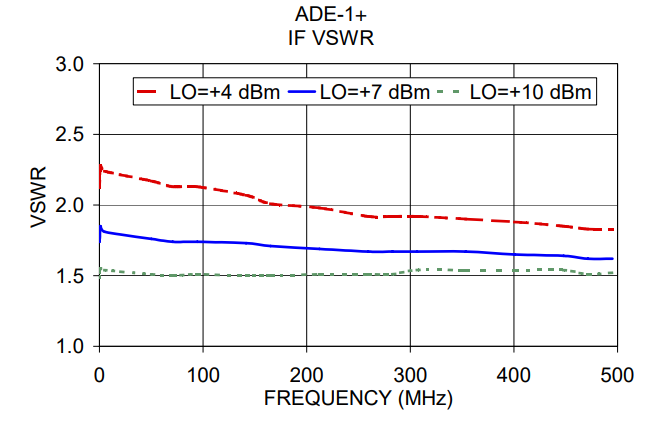
Port VWSR
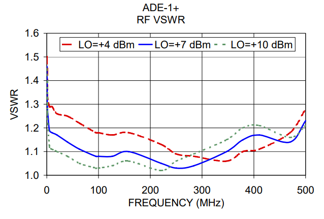
- Measured VSWR of 2.23 at 9 MHz with NanoVNA matches spec nicely
ADE-1 Measurements
NanoVNA Measurements
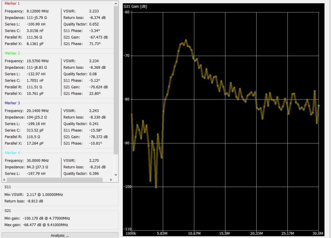
- No RF in
- LO driven by NanoVNA Tx
- About -10dBm output
- IF output to NanoVNA Rx
- IF at 9 MHz
- VSWR: 2.233
- S21 Gain: -67 dB
- NanoVNA
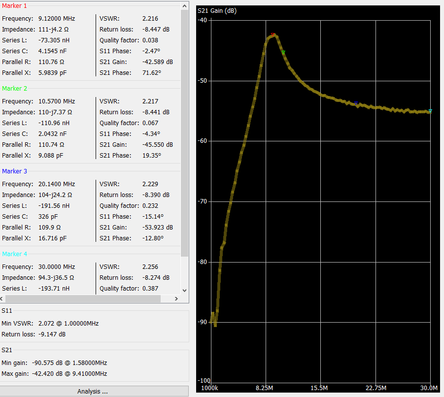
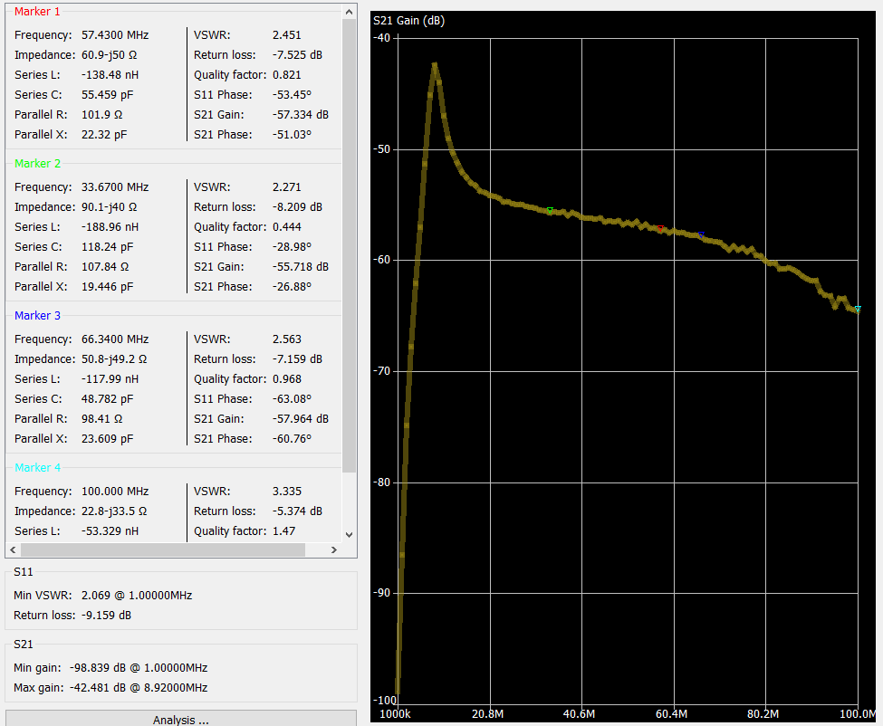
- No LO in
- RF driven by NanoVNA Tx
- IF output to NanoVNA Rx
- IF at 9 MHz
- VSWR: 2.216
- S21 Gain: -42 dB
- Scanning from 1 to 100 MHz
tinySA Measurements
LO to IF port isolation
- Driven by VFO-001 3.3V squarewave output
- Signal level about 0.5 dBm
- CLK0 = 9 MHz into LO port
- Monitor IF output from mixer on tinySA
- Output through 20 dB attenuator (tinySA set to -20dB gain)
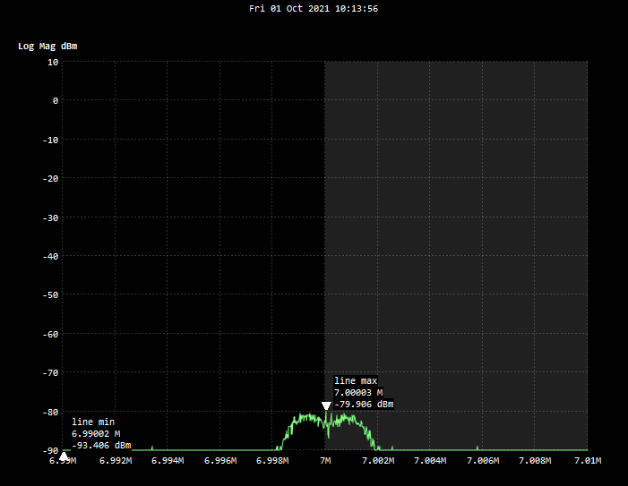
Mixer Operation
- Mixer is driven by VFO-001 3.3V squarewave outputs
- Signal output levels about 0.5 dBm
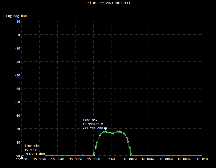
- CLK0 = RF @7 MHz VFO-001 output with 30 dB attenuator
- CLK1 = LO @16 MHz no attenuator
- Monitor IF output from mixer on tinySA
- IF out to tinySA with 20 dB attenuator (tinySA set to -20dB gain)
- Same but 9 MHz picked out
- Approx. 8 dB insertion loss
- Look at 7 MHz RF freq on IF output
- Look at 16 MHz LO freq on IF output
Typical Application
- 7 MHz RF, 40 M band
- 16 MHz LO
- Si5351A square wave drive
- 9 MHz (difference 16-7=9) IF feeds Crystal Filter
- SSB or CW Crystal Filter Design - 9 MHz nominal
- Use Si5351 to drive LO and/or RF ports
Si5351A Drive Level
- Si5351A used to drive LO and/or RF ports
- 3 outputs
- LO at full level (+7dBm)
- RF at various levels with attenuators to drop to expected RF signal levels
- Don't want more than 7 dBm into LO or RF ports
- Two Si5351 Designs to drive ADE-1 LO or RF ports
VFO-001 drive
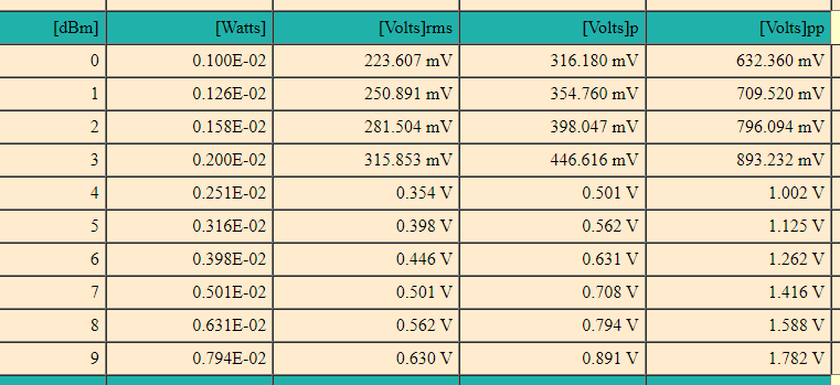
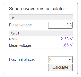
- The RMS value is for square-wave voltages whose pulse duration (ti) and pause (tp) have the same length:
- Drive level of 3.3V
- 100 mW is 20 dBm
- ADE-1 needs 7 dBm level
- Would need a 13 dB attenuator
- Not actually true
- Although the Si5351 datasheet says it drives 50 Ohms loads this is not exactly the case
- Drive levels are controlled by the output current setting
- Not actually true
- Si5351A outputs measured on VFO-001
- Drive Level 2 mA = 0.2 dBm
- Drive Level 4 mA = 6.2 dBm << Use this level
- Drive Level 6 mA = 9.7 dBm
- Drive Level 8 mA = 11.7 dBm
VFO-003 drive
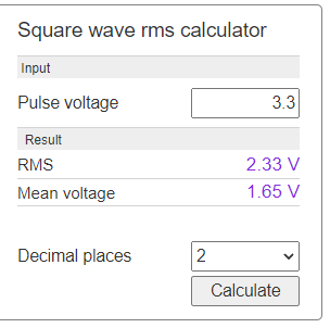
- RMS Voltage of square wave
- Square Wave Calculator
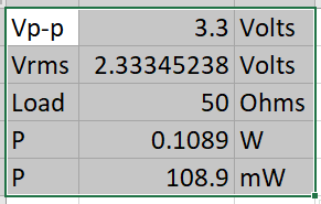
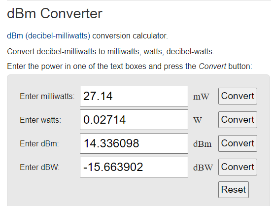
- 2.33V^2/100 = 0.0542W
- Power is split between Source and load resistors
- 0.02714W
- dBm Calculation
- Expect 14.3 dBm drive
- Measured 12.6 dBm with NanoVNA - Pretty close
- Need a 6 dB attenuator on the LO input to reduce VFO-003 for Level 7 mixers (like the ADE-1 mixer)
- 6 dB 150-36-150
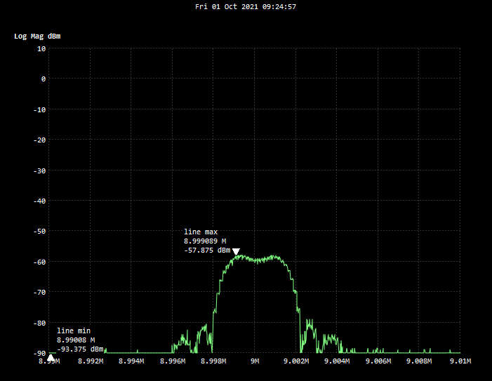
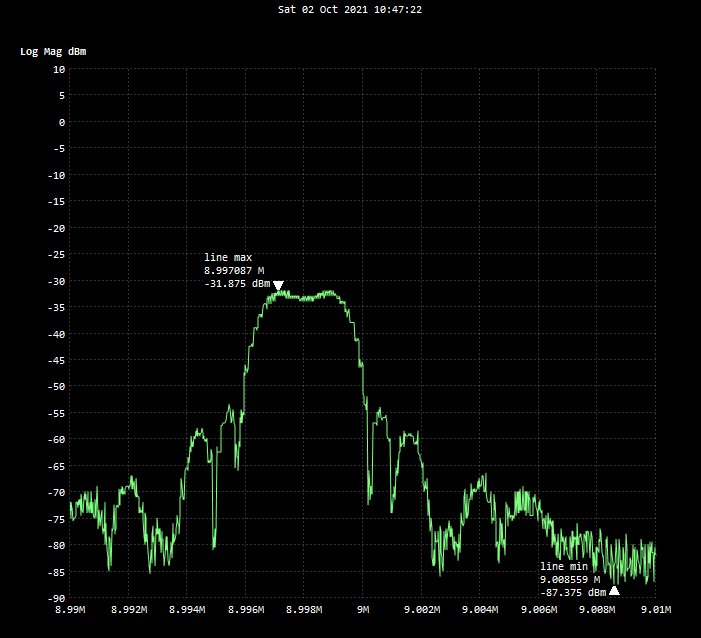
Mixer with SSB4 IF Crystal Filter
- Mixer is driven by VFO-001 3.3V squarewave outputs
- Signal output levels about 0.5 dBm
- CLK0 = RF @7 MHz VFO-001 output with 20 dB attenuator
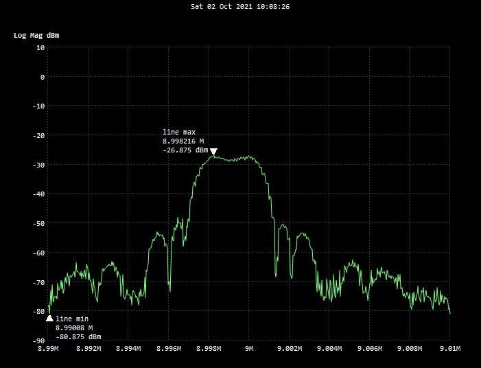
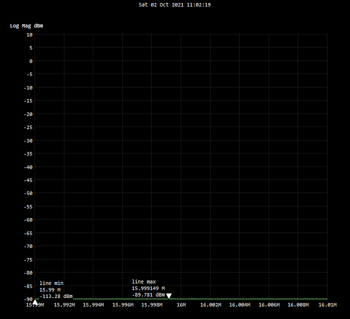
- CLK1 = LO @15.998,6 MHz no attenuator
- Adjusted to center of the SSB4 Crystal filter
- IF output from mixer to SSB4 Crystal filter input
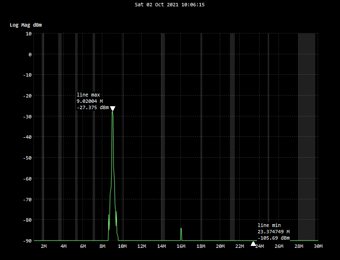
- Monitor SSB4 Crystal filter output on tinySA
- No attenuator on IF output into tinySA
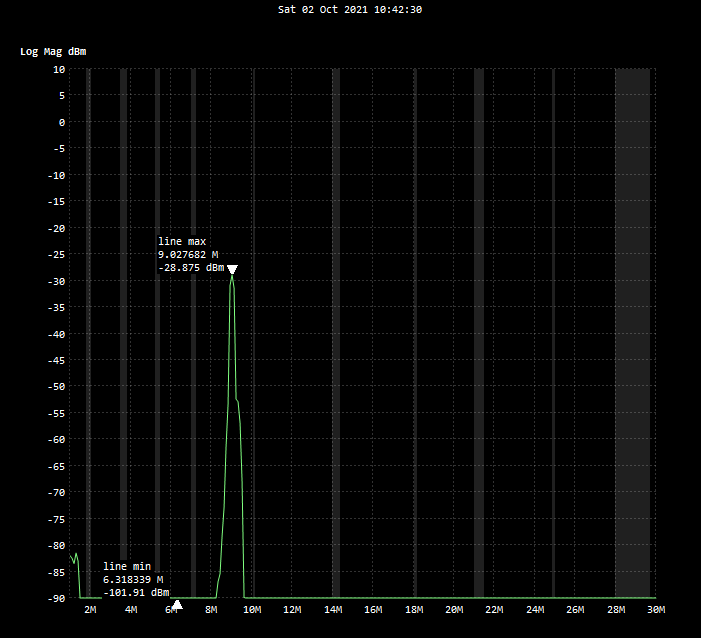
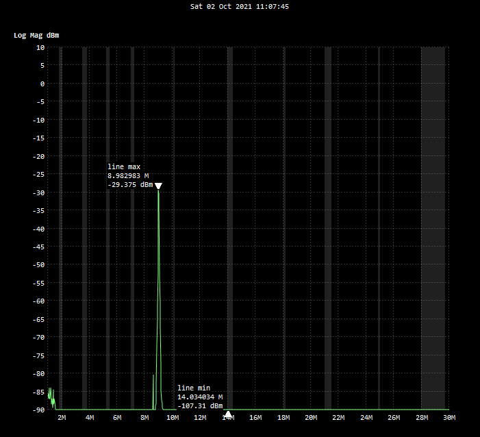
- Scan from 1 to 30 MHz
- Note other signals are now well into the noise floor of the tinySA
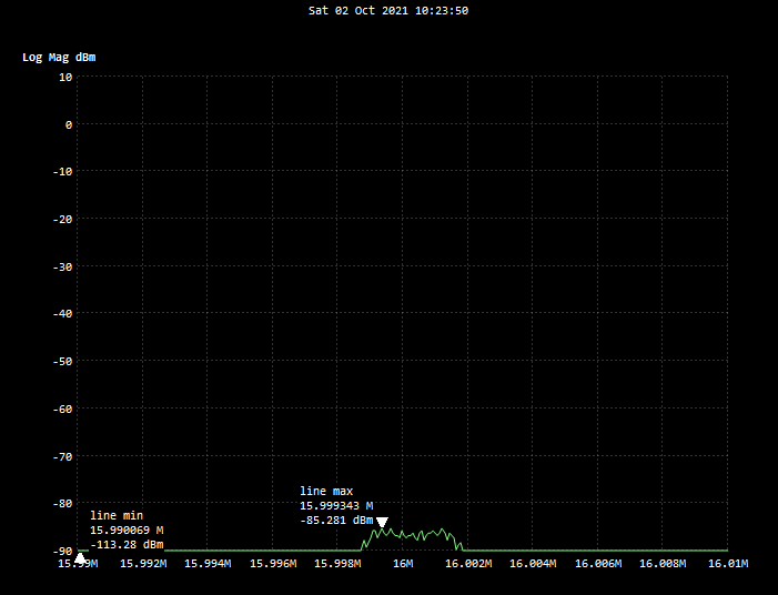
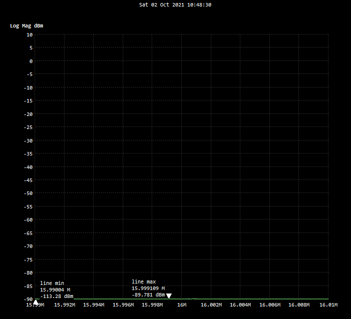
- LO present but down
- 16 MHz LO level
- 16 dB lower with crystal filter
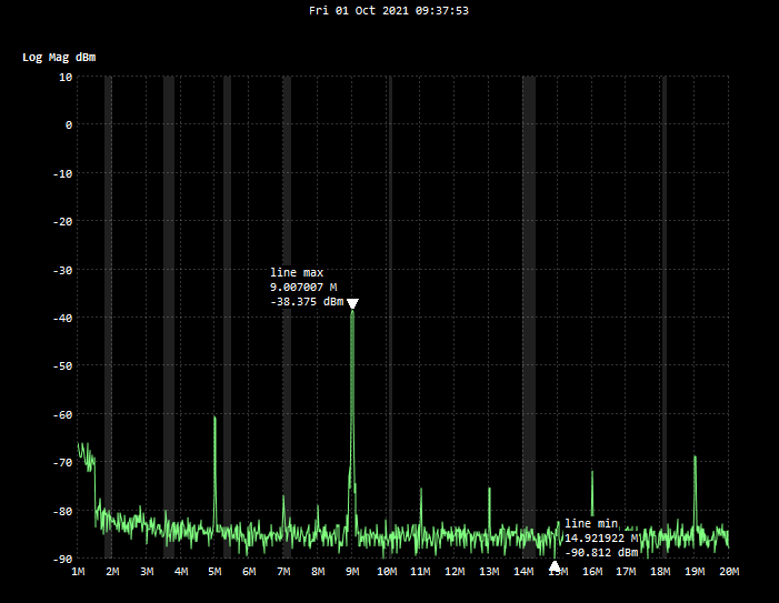
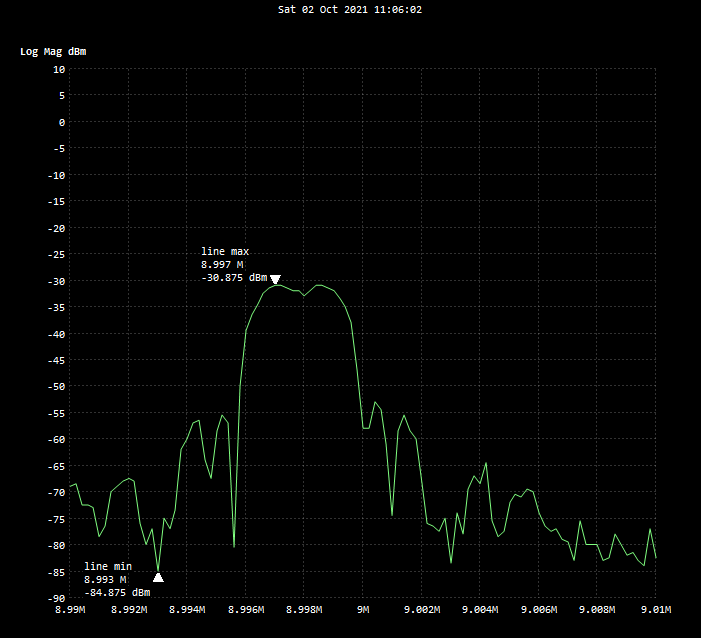
Mixer with CW5 IF Crystal Filter
- Mixer is driven by VFO-001 3.3V squarewave outputs
- Signal output levels about 0.5 dBm
- CLK0 = RF @7 MHz VFO-001 output with 20 dB attenuator
- CLK1 = LO @15.997,9 MHz no attenuator
- Adjusted to center of the CW5 Crystal filter
- IF output from mixer to CW5 Crystal filter input
- Monitor CW5 Crystal filter output on tinySA
- No attenuator on IF output into tinySA
- Scan from 1 to 30 MHz
- Note other signals are now well into the noise floor of the tinySA
- LO present but down
- 16 MHz LO level
- 16 dB lower with crystal filter
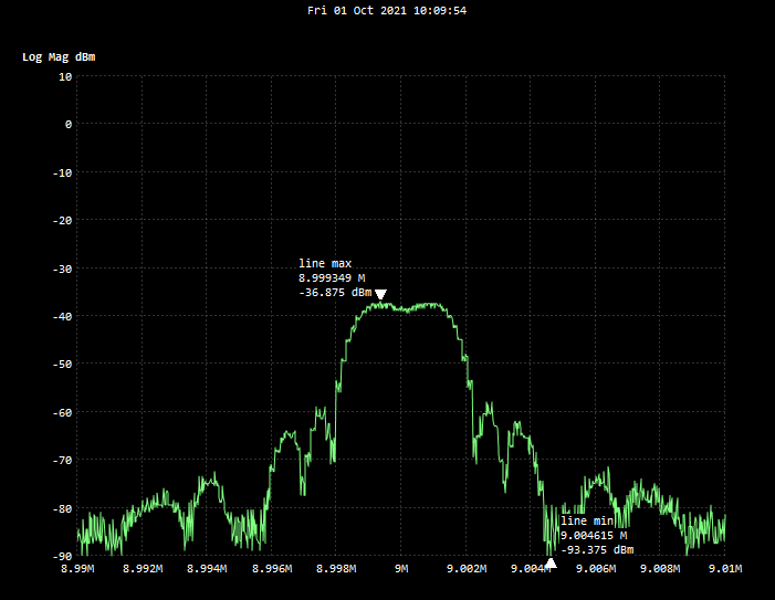
Mixer with CW3 IF Crystal Filter
- Mixer is driven by VFO-001 3.3V squarewave outputs
- Signal output levels about 0.5 dBm
- CLK0 = RF @7 MHz VFO-001 output with 20 dB attenuator
- CLK1 = LO @15.997,7 MHz no attenuator
- Adjusted to center of the CW3 Crystal filter
- IF output from mixer to CW3 Crystal filter input
- Monitor CW3 Crystal filter output on tinySA
- No attenuator on IF output into tinySA
- Scan from 1 to 30 MHz
- Note other signals are now well into the noise floor of the tinySA
- LO present but down
- 16 MHz LO level
- 16 dB lower with crystal filter
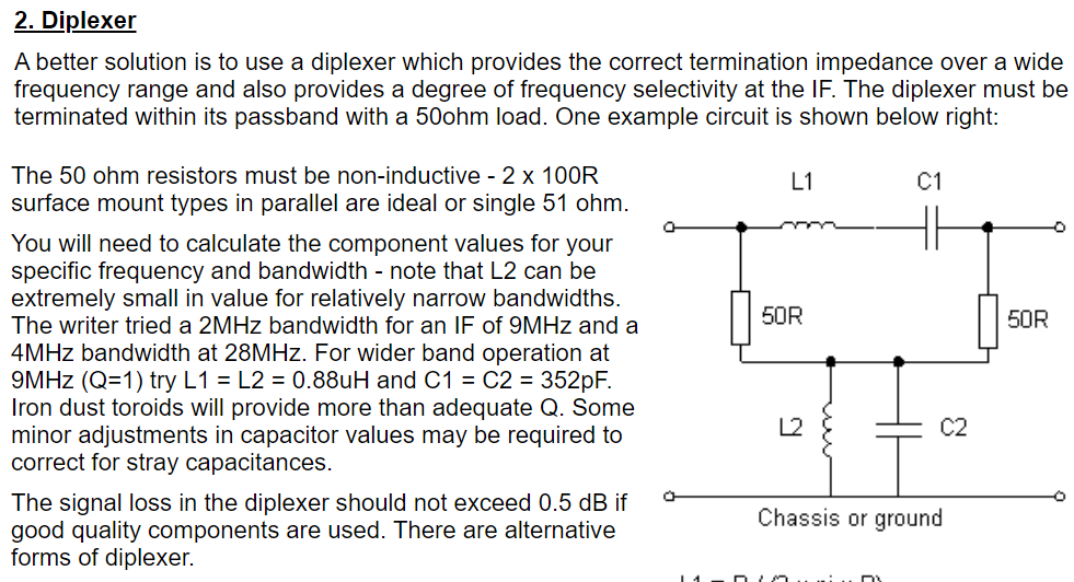
Bridged Tee Diplexer
Diplexor is a bandpass/band-stop filter popularized by Joe Reisert W1JR that is used after a double Balanced Mixer to provide a 50 ohm termination to all frequencies at the mixer's IF port, and to the following amplifier stage. Maintaining a consistent load at the mixer avoids overload and Inter-Modulation Distortion (IMD) effects that these mixers are prone to when not properly terminated.
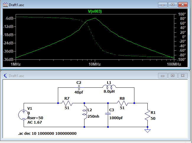
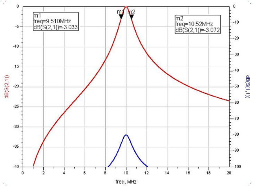
LTSpice simulation
- 9 MHz
- FT37-67, 20T-12" = 8 uH
- T37-17, 13T-10" = 250 nH
- C2 adjusts peak from left to right
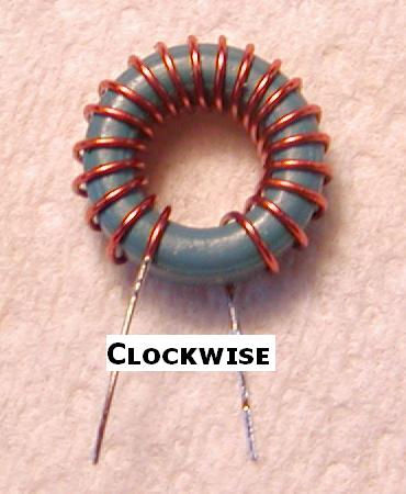
Toroid Winding Direction
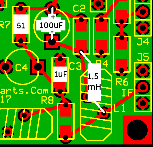
- Toroids needs to be wound to match the pad locations/offsets on the PCB
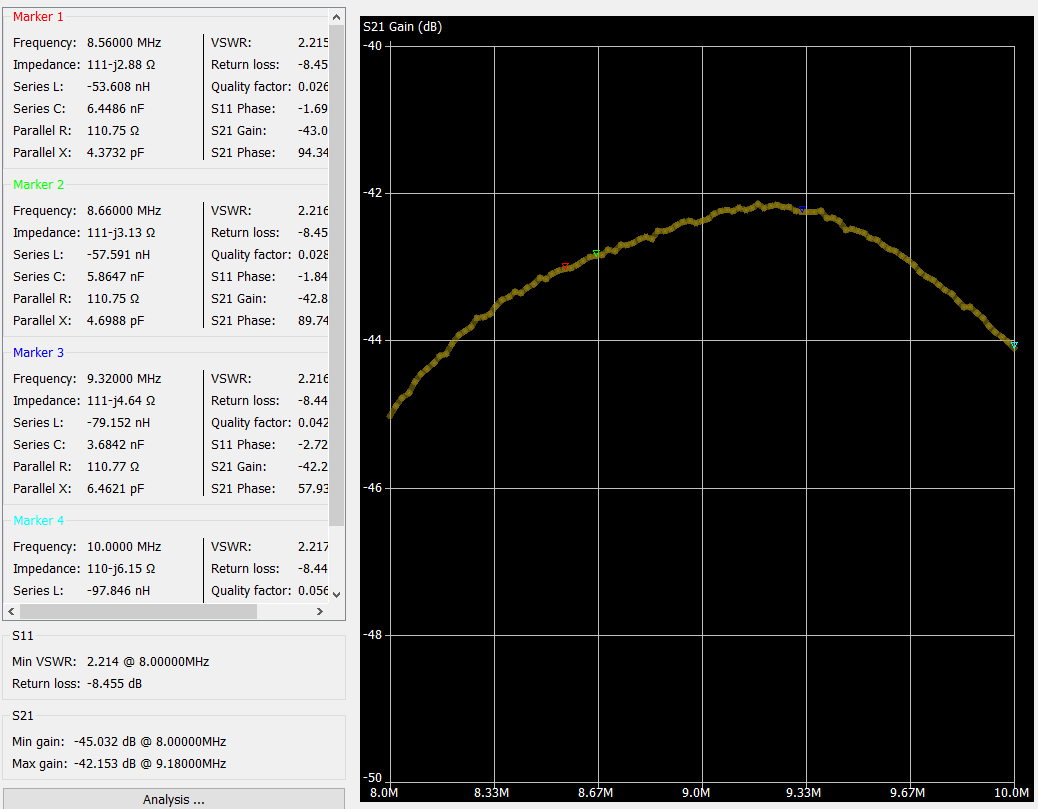
Adjust IF Diplexer C1 (ADE-1)
- Drive RF port from NanoVNA
- Nominal 0 dBm drive level
- IF port is output
- Listen on IF port on NanoVNA
- No drive on LO
- 9 MHz is IF design frequency
- Nano VNA set to scan from 1 Mhz to 30 MHz
- Shows peak expected signal around 9 MHz
- Scan from 8 to 10 MHz
- Adjust C1 to peak near 9 MHz
- Eliminate double peaks
ADE-1 Mixer as Product Detector
- RF is 9 MHz from IF stage
- LO is 9 MHz BFO from VFO-003
- Minor adjustments to get to side of the base band offset
- IF output is audio
- Mixer goes down to DC
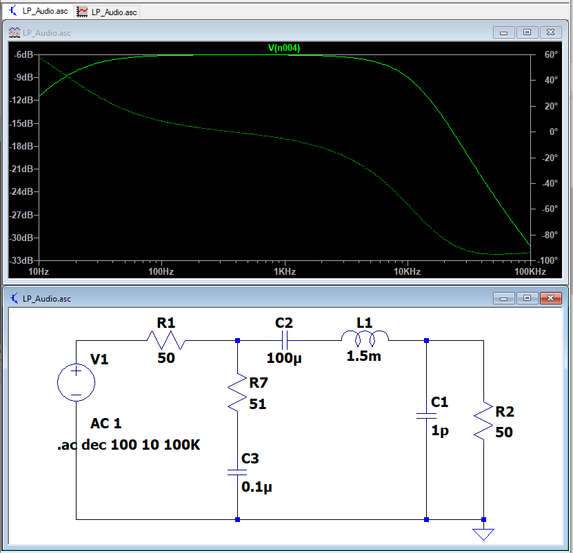
- IF needs Audio Filter
- IF port wants to see 50 Ohm termination across output
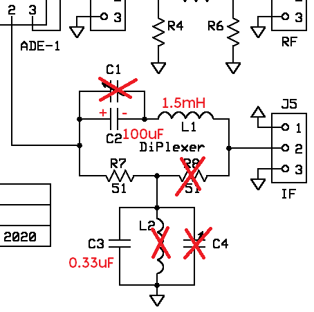
- 0.33 uF cap/50 ohms terminates higher frequencies at 50 ohms
- 1.5 mH inductor in series as filter on audio output
- LTSpice Simulation
- Circuit Mods
- IF section
Videos
