RF-Amp
Contents
RF Amplifier Features
- From Charlie Morris' (ZL2CTM) Go QRP Portable SSB Rig
- Solid State Design for the Radio Amateur?
- +22 dB gain
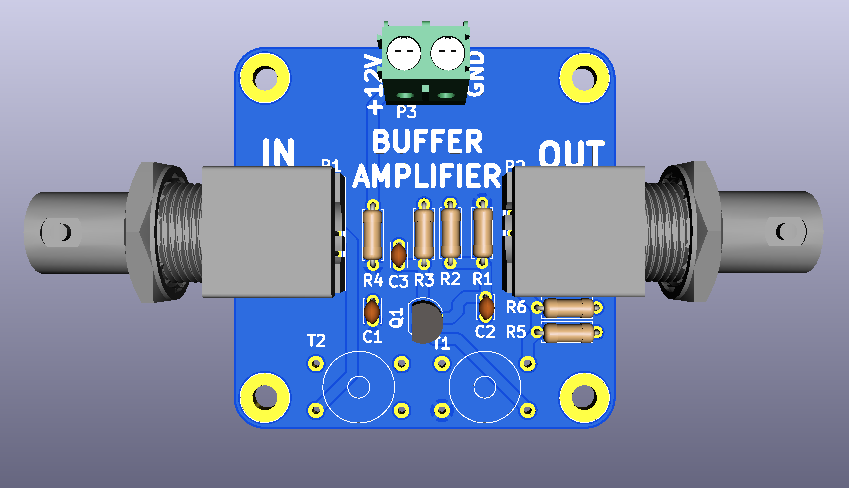
- Input connectors: SMA or BNC
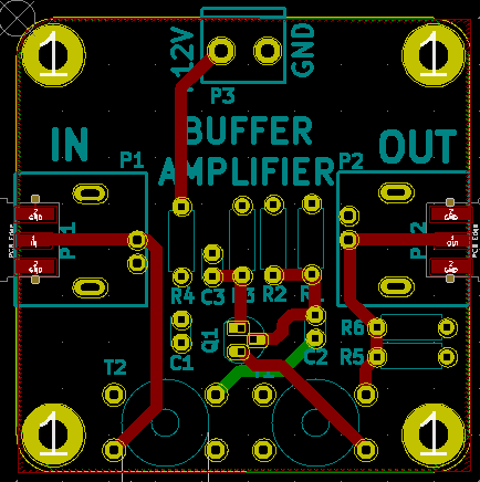
- 49x49mm card
- 4x 4-40 mounting holes
RF Amplifier Design
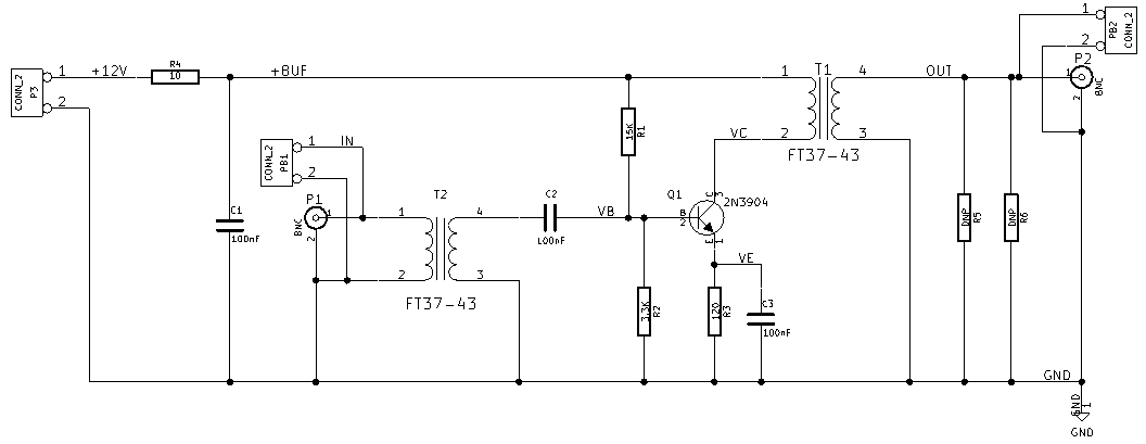
Schematic
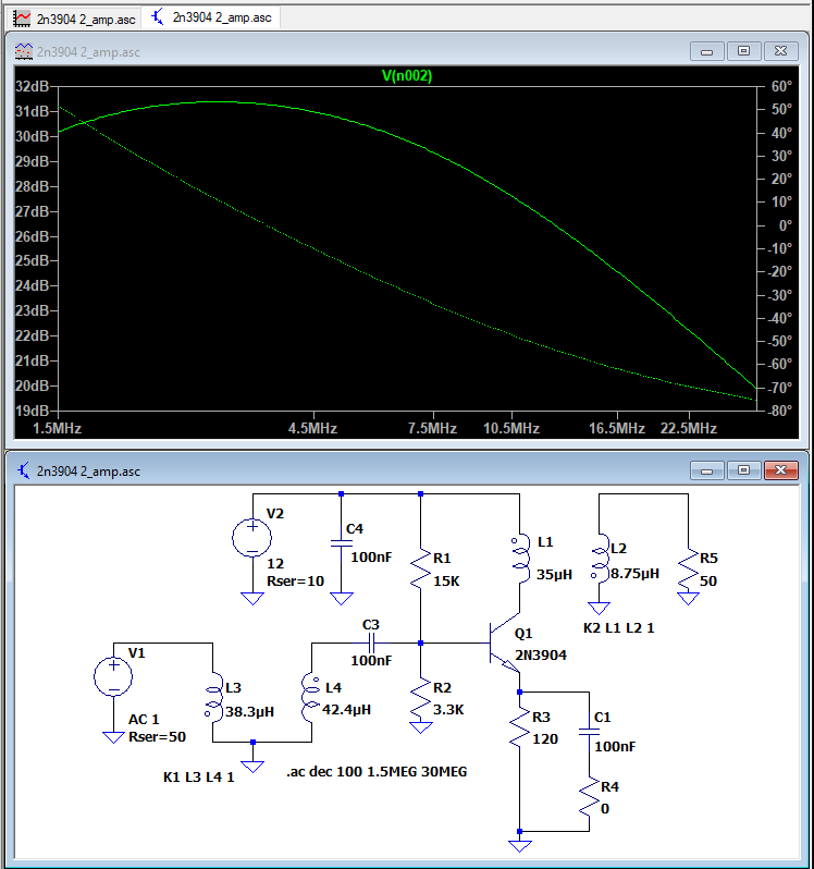
LT Spice Simulation
- LTspice Simulation - GitHub source file
- +28.4 dB at 9 MHz
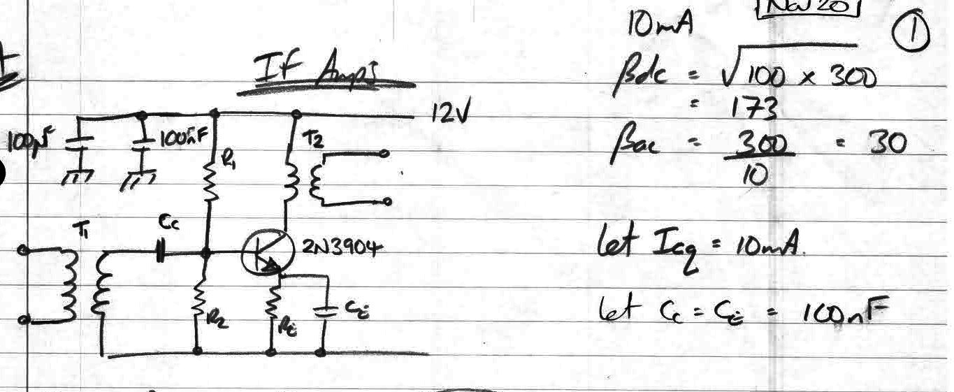
Charlie Morris Design
- From Charlie's notes with mods for my use
- 2N3904 data sheet
- Emitter Resistance - helpful paper
Beta DC
- Geometric mean min/max beta at operating current
- =sqrt(100*300) = 173
Beta AC
- Gain bandwidth product divided by operating frequency
- Assume operating frequency of 10 MHz (my IF is actually at 9 MHz)
- = 300/10 = 30
DC Operating Point
- CE current 10 mA
- If Vce = 6V, this is 60 mW power dissipation
- Assume Ve (voltage across emitter resistor) = 1/10 Vcc = 12V/10 = 1.2V
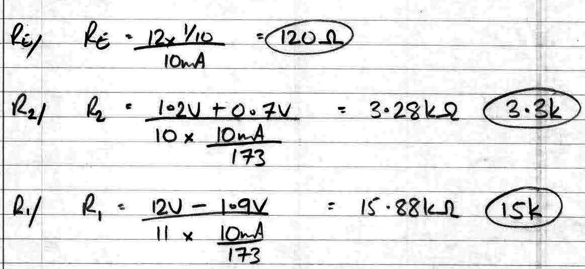
- R3 is Re (emitter resistor) = 1.2V/0.01A = 120 ohms
- VCE = 0.7V (typical from data sheet)
- V(emitter) = 1.2V
- V(base) = V(emitter) + VCE = 1.9V
- Assume current in biasing resistors = 10x current needed by DC beta
- 10 mA in C-E, beta DC less = 10 mA/173 = 48 uA
- 10x the current in the biasing resistors = 480 uA (calculated)
- R2 is 1.9V at 480 uA = 3.9K use 3.3K
- Actual current will be 1.9V/3.3 ohms = 634 mA
- R1 sources current to R2 and transistor base
- Voltage = Vcc (12V) - 1.9V = 10.1V
- Current = 576 uA + 57 uA = 634 uA
- R1 = 10.1 / .634 mA = 15.9K, use 15k
Input resistance
- Xc for 0.1uF cap from emitter to ground
- C=0.1uF
- F=10MHz
- 1/2*pi*F*C = 0.16 ohms
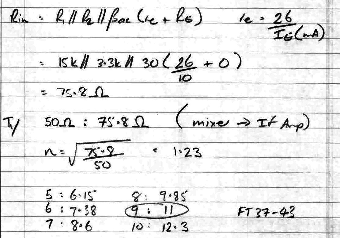
- Parallel resistors R1, R2 paralleled with transistor input impedance
- R1=15K, R2=3.3K
- Transistor resistance = Beta AC (30) times re
- re = 26 / Ie (10 mA in mA) = 26/10 = 2.6
- Beta AC * re = 30*2.6 = 78 ohms - predominates
- All in parallel are 75.8 ohms
Input/Output Transformers
Tracks
Input Transformer
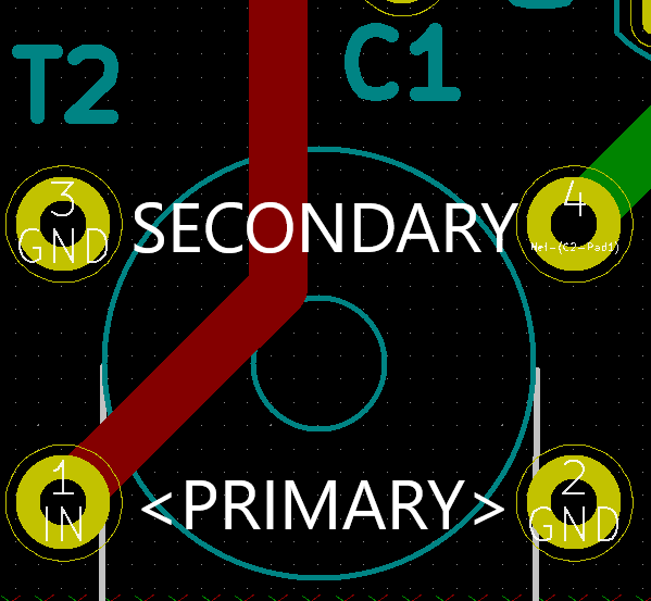
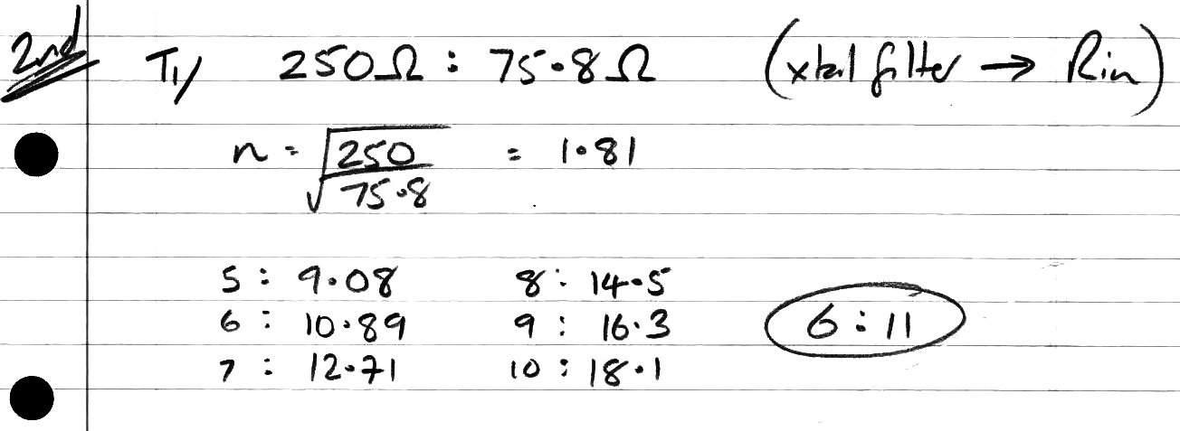
- Input Transformer (T1 on Charlie's - T2 on this board)
- 50:75.8 Ohms = 1 : 1.23 turns ratio
- n = sqrt(Zout/Zin) = sqrt(75.8/50) = 1.23
- 9:11 = 1:1.22 (close enough)
- 9 turns primary
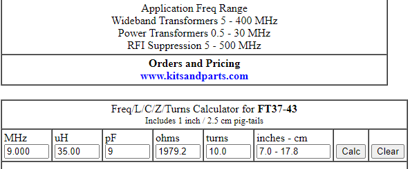
- 9 turns on FT37-43 = 38.3 uH
- 11 turns on secondary
- 11 turns on FT37-43 = 42.4 uH
- 20 turns = 12 in
Output Transformer
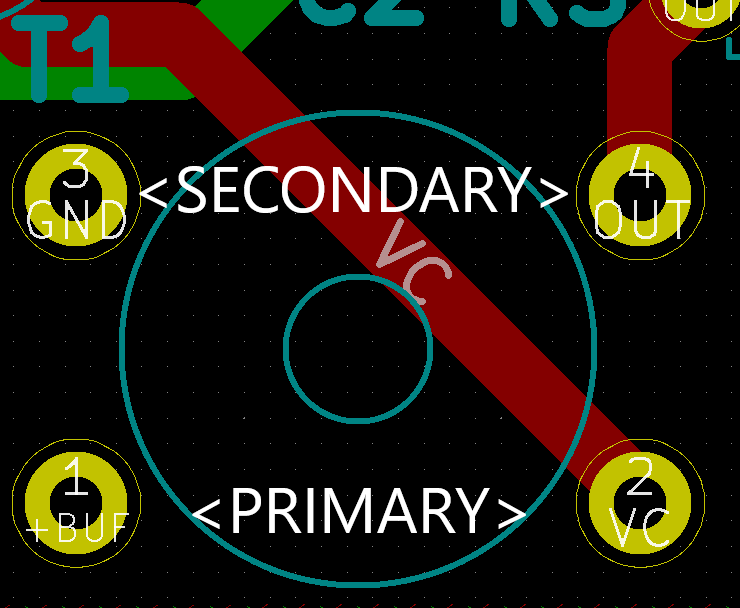
- Output transformer (T2 on Charlie's - T1 on this board)
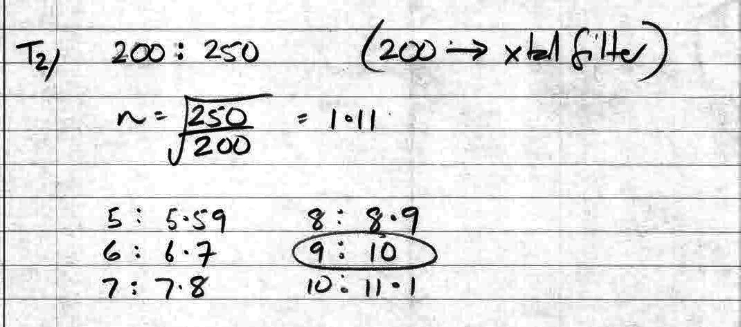
- T2 - different than Charlie's design since my Crystal filters are all 50 ohms in/out
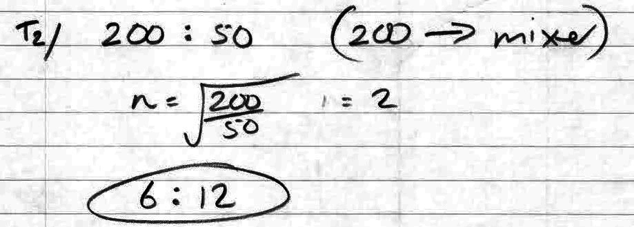
- 200:50 ohms
- n = sqrt(200/50) = 2:1
- 10:5 turns
- 10 turns primary (on transistor collector)
- 10 turns = 35 uH
- 5 turns secondary (towards output)
- 5 turns = 8.75 uH
- 10 turns primary (on transistor collector)
- 8 15 turns = 9.5 in
Charlie's Notes
NanoVNA Measurements
- Goal: Attempt to measure RF-Amp performance using a [NanoVNA]] running NanoSaver software on PC
- S21 (gain) need to be measured with a 40 dB attenuator on input to avoid compression on the output
- S11 (reflection) input impedance can't be measured with input attenuator because S11 just ends up measuring the attenuator
- Output should be terminated to 50 ohms for S11 measurement
Measure S21
- Put 40 dB attenuator on input, measure S21
- Measure S21 with 9:11 input transformer
- Is there compression on lower frequencies?
- Set external attenuator to 40 dB using RF Attenuators
- DC current = 12 mA
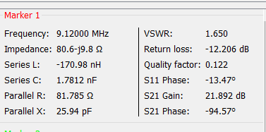
- At 9 MHz IF Frequency
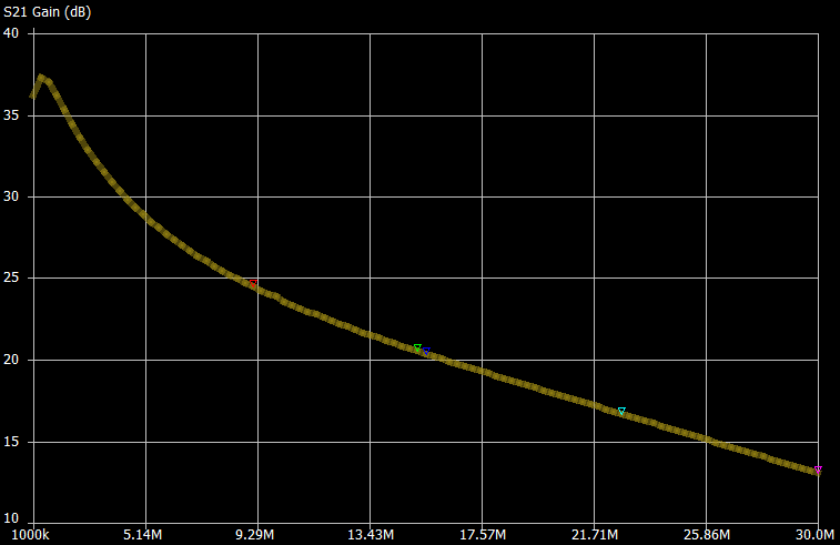
- S21 Gain = +22.4 dBm
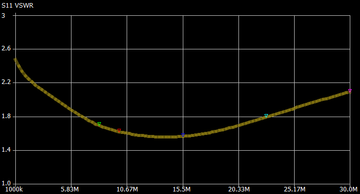
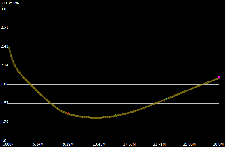
- VSWR = 1.64
- Input impedance = 76.6-j13 ohms
- S21 = +20 dBm at 15.5 MHz
Tweeks to design
- Moved 40 dB attenuator to right side, should be from NanoVNA output into RF-Amp card input
- Compressing/expanding output transformer doesn't change result much
- Compressing/expanding input transformer changes VSWR resonant frequency and S21 quite a bit
- Input isn't close enough to 50 Ohms
- Adjust input transformer ratio?
- Removed 2 windings on input to reduce input impedance
- Very good results
- +24.4 dBm gain at 8 MHz
- Terminate RF-AMP and measure VWSR
Video
