EP2C5-DB
Contents
EP2C5-DB-TH FPGA card
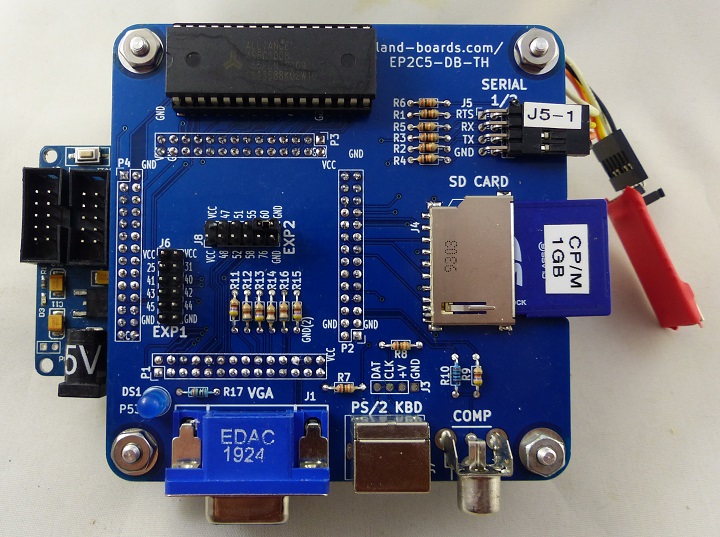
I love Grant Searle's Multicomp project. It lets you easily create 6502, Z80, 6809 Retrocomputers of the late 1970s era. This card provides all of the connections needed.
Grant's original design used an EP2 and that's exactly what this cards USES. Note that's not compatible with the latest version of Altera/Intel Quartus but you can download older versions like 13.1 SP1. Just make sure it supports the Cyclone II family of FPGAs.
We also have two EP4 versions of this card for sale on Tindie (bare board, you populate).
Features
- Full MultiComp Support of classic 8-bit Retrocomputers
- Mounts Cyclone II EP2C5 Mini Dev Board
- EP2C5T144C8N FPGA Card - Ebay listing
- 6 bit video on VGA (2:2:2 R:G:B)
- 128KB of SRAM for banked use in CP/M
- PS/2 Keyboard Mini-DIN connector
- Connector for serial ports
- Can attach inexpensive FTDI USB to serial converter
- Supports hardware handshake for high speed serial
- SD Card
- DC power jack (on FPGA card)
EP2 Resources
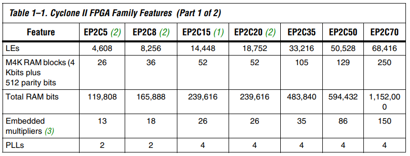
- EP2C5 has 26 of 512x9 SRAM blocks
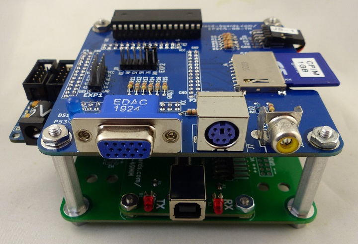
Stackup with FTDI Card
- Top to bottom of stackup
- EP2C5-DB (this card)
- Cyclone II EP2C5 Mini Dev Board
- FTDI-49MM
- CARRIER 95mm TO 49MM
Hardware
- 4-40 screws with nuts as spacers between CARRIER 95mm TO 49MM and FTDI-49MM
- (4) 1.25" tall, 6-32 M-F Standoffs FC4546-632-A connect CARRIER95TO49MM to EP2C5-DB
- (4) 1/4" tall, 6-32 M-F Standoffs FC4536-632-A as spacer below CARRIER95TO49MM board
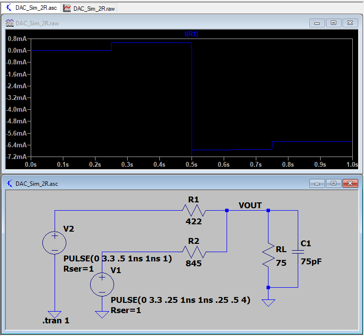
VGA - Ideal Drive 2:2:2 Case
- FPGA has a 3.3V driver which can drive 8 mA
- Ideal case drive current
- 0.7V into 75 Ohms = 9.33 mA
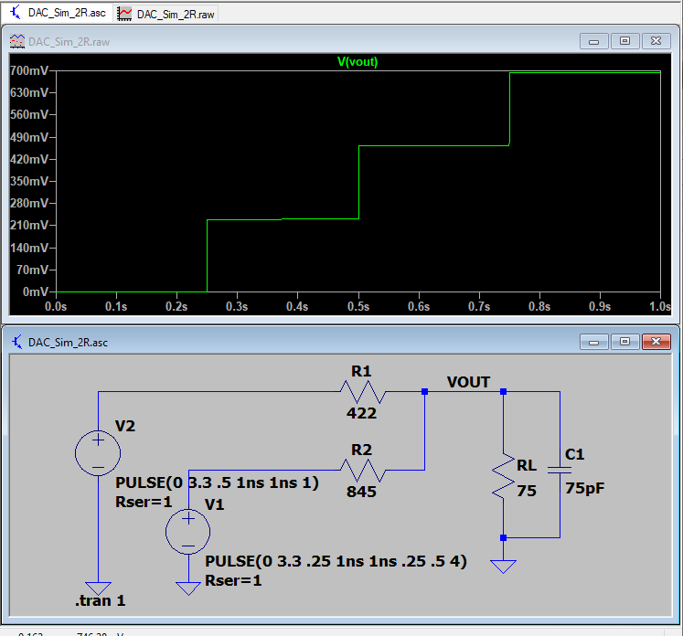
- R-2R values
- Ideal resistor values are 417.9 ohms and 835.7 ohms
- Standard value 1% resistors
- 1% standard values are 422 (Mouser), 845 (Mouser) Ohms
- Get closest values
- 0V, 0.228V, 0.460V, 0.693V
- Voltage steps are:
- Current steps are:
LEDs
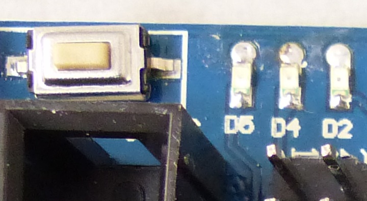
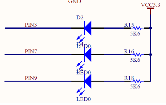
LEDs on EP2C5 Board
- D2 is on PIN_3
- D4 is on PIN_7
- D5 is on PIN_9
LED on EP2C5-DB Cards
- LED is on FPGA pin 53
Connectors
J1 - VGA
J4 - SD Card
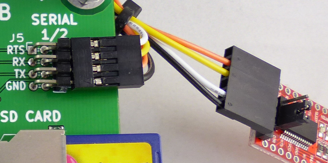
J5 - Serial Ports 1/2
- Set jumper on FTDI module to 3.3V
- Connects to FTDI Module
- RTS
- RXD
- TXD
- GND
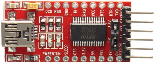
FTDI Module
- Set jumper on FTDI module to 3.3V
FTDI Wiring
- Set jumper on FTDI module to 3.3V
- J5-1 (marked RTS on PCB) to FTDI CTS pin
- J5-3 (marked RX on PCB) to FTDI TX pin
- J5-5 (marked TX on PCB) to FTDI RX pin
- J5-7 (marked GND on PCB) to FTDI GND pin
J6 - 8-bit I/O connector
- FPGA Pins
- 3.3V
- 3.3V
- 25
- 31
- 41
- 40
- 43
- 42
- 45
- 44
- GND
- GND
J8 - 8-bit I/O connector
- FPGA Pins
- 3.3V
- 3.3V
- 48
- 47
- 52
- 51
- 58
- 55
- 76
- 69
- GND
- GND
Schematics
Retro-Computer Builds
- Github repository for Multicomp builds
- M6502 CPU, OSI BASIC-in-ROM, VGA, PS2, External RAM
- UK101, Grant Searle's Original, CEGMON and BASIC-in-ROM
- UK101, 4K SRAM, CEGMON and BASIC-in-ROM
- UK101, NTSC, PS2, Ext SRAM, CEGMON and BASIC-in-ROM
- UK101, VGA, PS2, External SRAM, 115200 baud Serial, CEGMON and BASIC-in-ROM
- M6800, MIKBUG ROM
- M6800, MIKBUG ROM, External RAM
- M6800, MIKBUG ROM at 0xF000 base, External RAM
- M6800, MIKBUG ROM, Serial port
- M6809, 56K SRAM, VGA
- Z80, CP/M 2, VGA, PS2, 128K SRAM
- Z80, CP/M 2, VGA, PS2, 128K SRAM
- PDP-8 4KW, Serial, VGA
Programming the Flash EPROM Memory
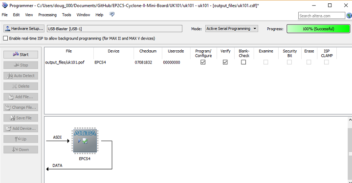
Permanent (.pof file)
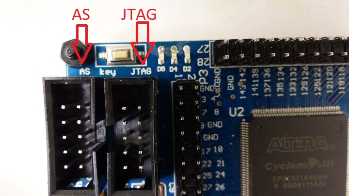
- AS - Upload ,pof file to EPROM over AS
- Flash EPROM = EPCS4
- Remains after power cycling
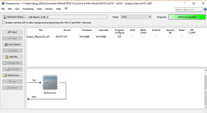
Temporary (.sof file)
- JTAG - Upload temporary .sof program over JTAG
- Does not remain after power cycling
Pin List (Multicomp)
# Clocks and reset
set_location_assignment PIN_17 -to clk
set_location_assignment PIN_144 -to n_reset
set_instance_assignment -name WEAK_PULL_UP_RESISTOR ON -to n_reset
# PS/2
set_location_assignment PIN_87 -to ps2Data
set_location_assignment PIN_86 -to ps2Clk
# ACIA (Serial)
set_location_assignment PIN_60 -to serSelect
set_instance_assignment -name WEAK_PULL_UP_RESISTOR ON -to serSelect
set_location_assignment PIN_104 -to urts1
set_location_assignment PIN_101 -to urxd1
set_instance_assignment -name WEAK_PULL_UP_RESISTOR ON -to rxd1
set_location_assignment PIN_103 -to utxd1
# External SRAM
set_location_assignment PIN_4 -to n_sRamWE
set_location_assignment PIN_126 -to n_sRamCS
set_location_assignment PIN_134 -to n_sRamOE
set_location_assignment PIN_32 -to sramAddress[16]
set_location_assignment PIN_8 -to sramAddress[15]
set_location_assignment PIN_30 -to sramAddress[14]
set_location_assignment PIN_24 -to sramAddress[13]
set_location_assignment PIN_28 -to sramAddress[12]
set_location_assignment PIN_136 -to sramAddress[11]
set_location_assignment PIN_132 -to sramAddress[10]
set_location_assignment PIN_139 -to sramAddress[9]
set_location_assignment PIN_142 -to sramAddress[8]
set_location_assignment PIN_143 -to sramAddress[7]
set_location_assignment PIN_141 -to sramAddress[6]
set_location_assignment PIN_137 -to sramAddress[5]
set_location_assignment PIN_135 -to sramAddress[4]
set_location_assignment PIN_133 -to sramAddress[3]
set_location_assignment PIN_129 -to sramAddress[2]
set_location_assignment PIN_125 -to sramAddress[1]
set_location_assignment PIN_121 -to sramAddress[0]
set_location_assignment PIN_122 -to sramData[7]
set_location_assignment PIN_120 -to sramData[6]
set_location_assignment PIN_118 -to sramData[5]
set_location_assignment PIN_114 -to sramData[4]
set_location_assignment PIN_112 -to sramData[3]
set_location_assignment PIN_113 -to sramData[2]
set_location_assignment PIN_115 -to sramData[1]
set_location_assignment PIN_119 -to sramData[0]
# Composite Video
set_location_assignment PIN_75 -to video
set_location_assignment PIN_74 -to videoSync
# VGA
set_location_assignment PIN_64 -to videoB0
set_location_assignment PIN_63 -to videoB1
set_location_assignment PIN_67 -to videoG0
set_location_assignment PIN_65 -to videoG1
set_location_assignment PIN_70 -to videoR0
set_location_assignment PIN_69 -to videoR1
set_location_assignment PIN_71 -to hSync
set_location_assignment PIN_72 -to vSync
# SD Card
set_location_assignment PIN_92 -to sdMISO
set_instance_assignment -name WEAK_PULL_UP_RESISTOR ON -to sdMISO
set_location_assignment PIN_94 -to sdSCLK
set_location_assignment PIN_93 -to sdMOSI
set_location_assignment PIN_97 -to sdCS
set_location_assignment PIN_3 -to driveLED
# J6 IO
set_location_assignment PIN_25 -to J6IO8[0]
set_location_assignment PIN_31 -to J6IO8[1]
set_location_assignment PIN_41 -to J6IO8[2]
set_location_assignment PIN_40 -to J6IO8[3]
set_location_assignment PIN_43 -to J6IO8[4]
set_location_assignment PIN_42 -to J6IO8[5]
set_location_assignment PIN_45 -to J6IO8[6]
set_location_assignment PIN_44 -to J6IO8[7]
# J8 I/O
set_location_assignment PIN_48 -to J8IO8[0]
set_location_assignment PIN_47 -to J8IO8[1]
set_location_assignment PIN_52 -to J8IO8[2]
set_location_assignment PIN_51 -to J8IO8[3]
set_location_assignment PIN_58 -to J8IO8[4]
set_location_assignment PIN_55 -to J8IO8[5]
set_location_assignment PIN_76 -to J8IO8[6]
# set_location_assignment PIN_60 -to J8IO8[7]

