Kits and Parts Universal Wideband Small Signal RF Amplifier
Revision as of 15:23, 23 October 2021 by Blwikiadmin (talk | contribs)
Contents
Specs
- Kits and Parts Universal Wideband Small Signal RF Amplifier
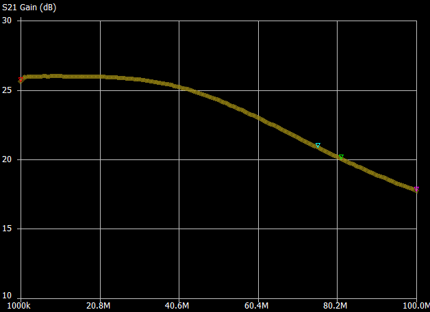
- Spec: 22+ dBm power gain from 2-30 MHz
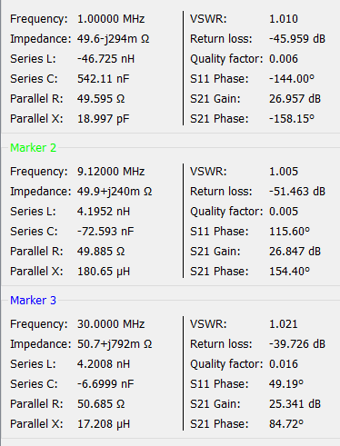
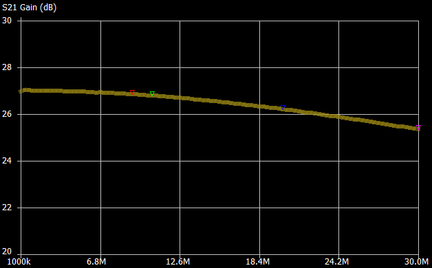
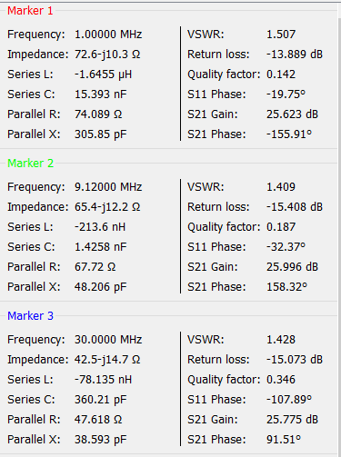
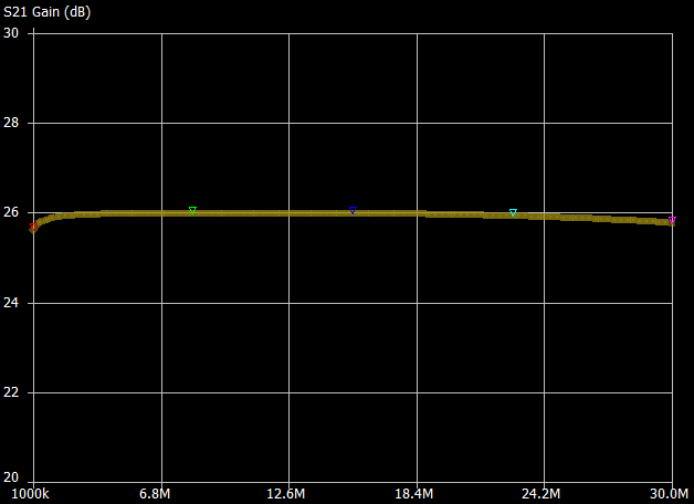
- Measured +25-27 dBm gain - fairly flat response
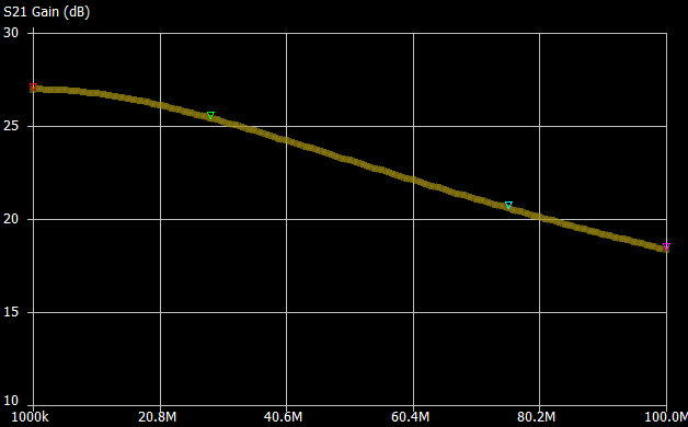
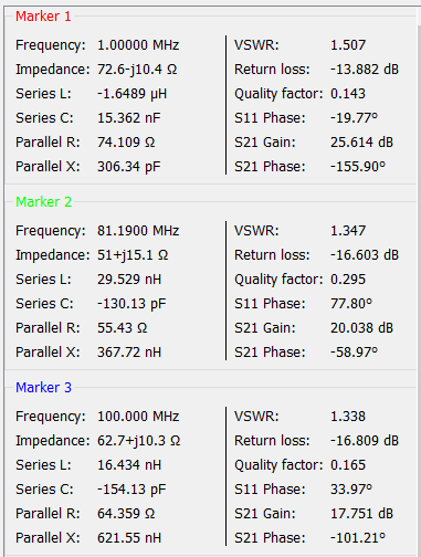
- +20 dBm gain up to 80 MHz
- 50 ohm input and 50 ohm output.
- 100 milliwatt maximum output.
- 0.031A at 12V = 370mW
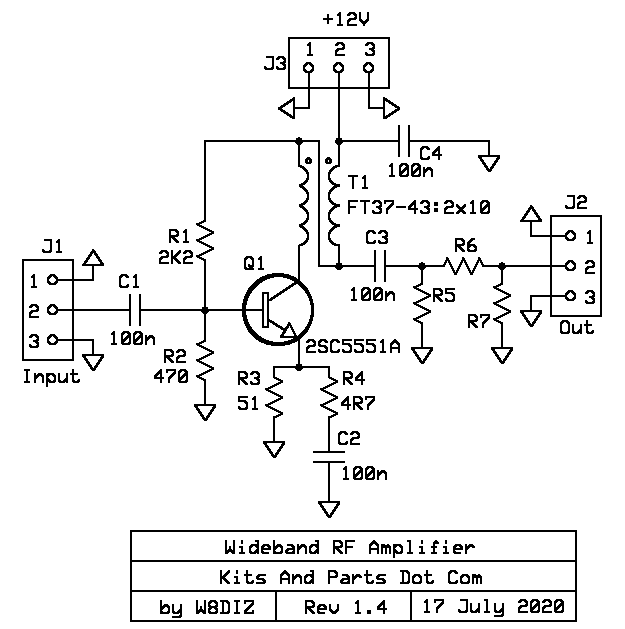
Schematic
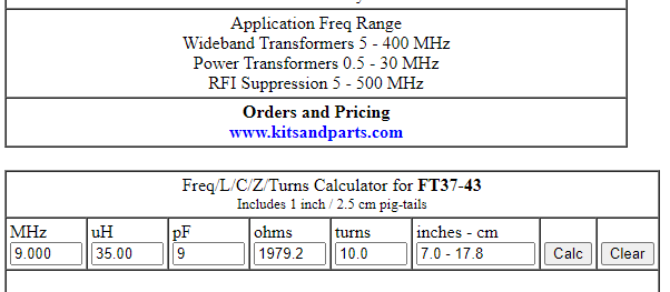
Transformer
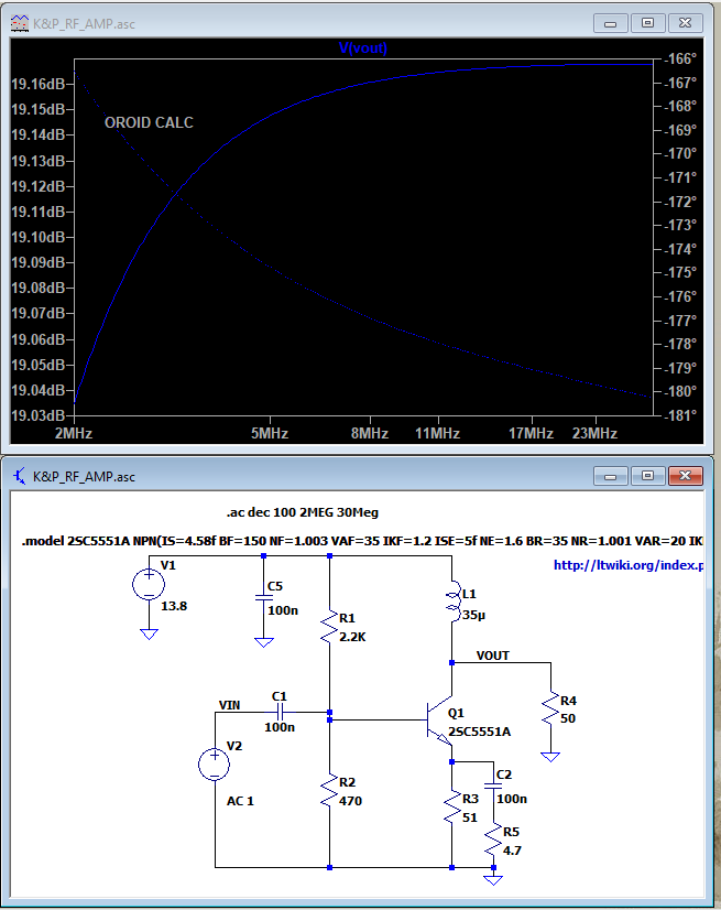
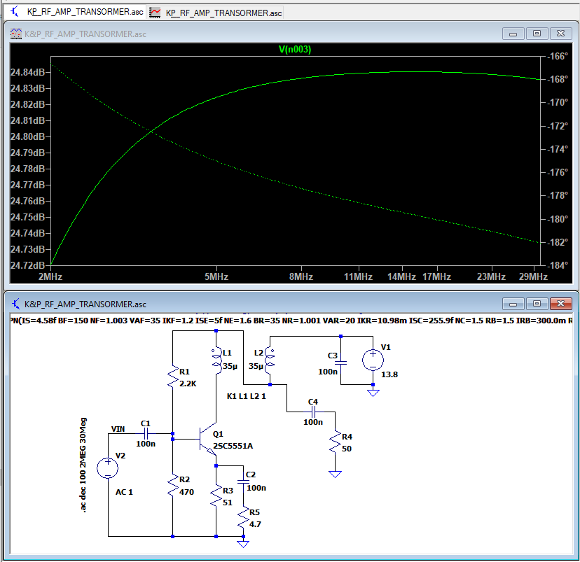
LTSPICE Simulation
.model 2SC5551A NPN(IS=4.58f BF=150 NF=1.003 VAF=35 IKF=1.2 ISE=5f NE=1.6 BR=35 NR=1.001 VAR=20 IKR=10.98m ISC=255.9f NC=1.5 RB=1.5 IRB=300.0m RBM=300m RE=280m RC=1.25 XTB=0 EG=1.11 XTI=3 CJE=2.36p VJE=199.0m MJE=73.20m TF=30.50p XTF=13.45m VTF=280.0m ITF=25.80m PTF=25.7 CJC=3.08p VJC=520.0m MJC=380.8m .15m TR=1.38n FC=1.51m )
- Without transformer
- With transformer
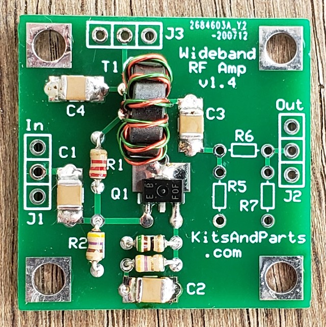
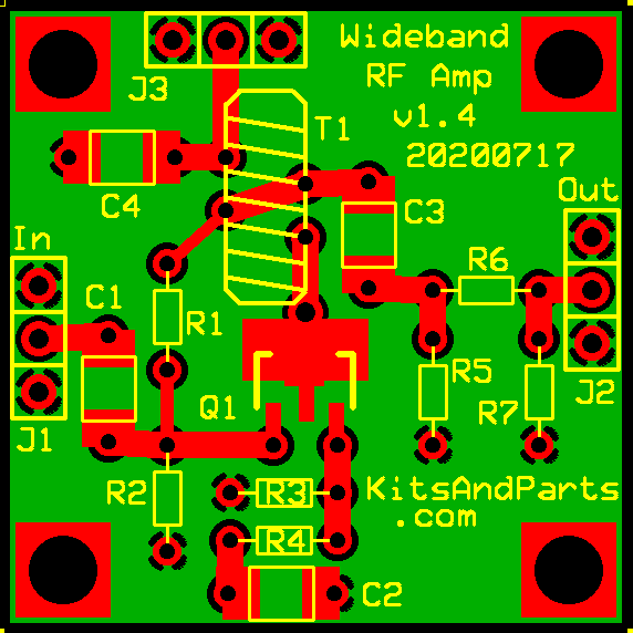
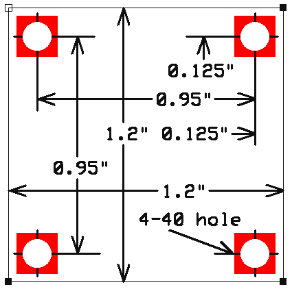
PCB
Build Instructions
- Align the SMD 2SC5551A RF Transistor onto Q1 pad in the center of the PCB. Using a temperature controlled solder pencil, solder without overheating.
- Align the four 100n SMD capacitors on the PCB and solder.
- Install resistors R1, R2, R3 and R4 on the PCB and solder.
- Install Toroids Transformer T1, Twist the Red & Green wires together to about 4 twists per inch. Wind 10 turns of the twisted wires onto the toroid. The magnet wire is heat stripable; trim each wire end to 3/4 inches. Prepare the toroid wires for soldering.
- Magnet Wire Soldering Details Here: One of each colored wires connects under the toroid and one of each colored wires connects on the outside of the toroid. One color wire should connect to J3/C4 and the other color connects to Q1. You should also have 2 different color wires connecting under the toroid via a PCB trace.
- R5,6,7 (not included) are used to attenuate the rf output. Place a jumper wire across R6.
- Connect the RF Amplifier via J1(input), J2(output) and J3(power).
NanoVNA Measurements
- Tried 30 dB Attenuator in and out sides of RF Amplifier with somewhat different results
Attenuator Before Amp
- NanoVNA
- Sweep settings, Attenuator in port CH1 (s21) in dB: 30.0
- Attenuator - 30 dB
- Below are with 30 dB attenuator between NanoVNA CH0 (output) and RF Amp input
- Built four Amplifier cards, identical results
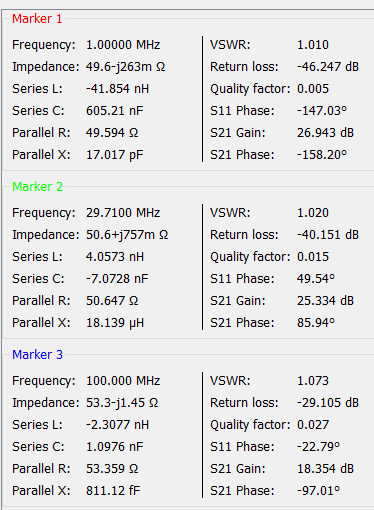
At 1, 9 and 30 MHz
- 30 dB attenuator between NanoVNA CH0 (output) and RF Amp input
S21 Gain
- 30 dB attenuator between NanoVNA CH0 (output) and RF Amp input
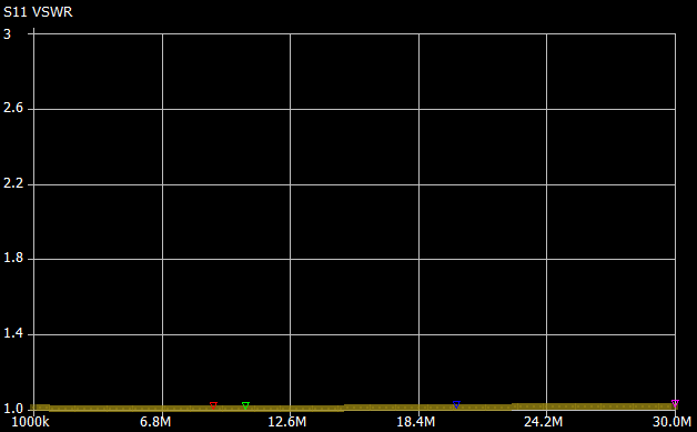
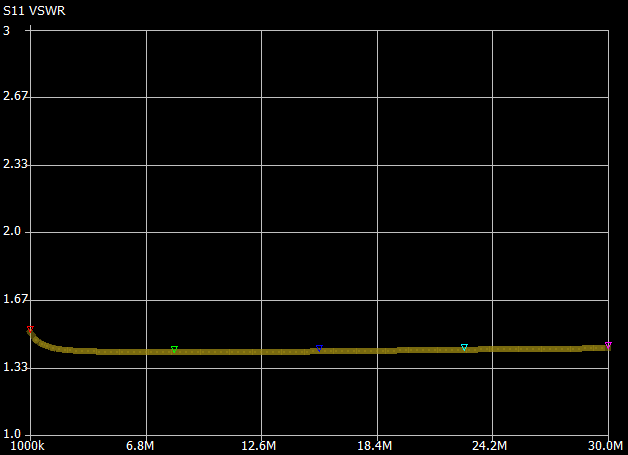
SWR
- 30 dB attenuator between NanoVNA CH0 (output) and RF Amp input
- Very good match into attenuator (as would be expecteed)
1-100 MHz Sweep
Attenuator After Amp
- 30 dB attenuator between NanoVNA CH0 (output) and RF Amp input
- 20 dB gain at 80 MHz
At 1, 9 and 30 MHz
- NanoVNA
- Repeated with 30 dB attenuator between RF Amp output and the NanoVNA CH1 (input)
- Attenuator - 30 dB
S21 Gain
- 1-30 MHz scan
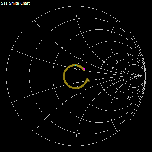
SWR
- Not as great (still OK) match into actual input (without attenuator)
