Features
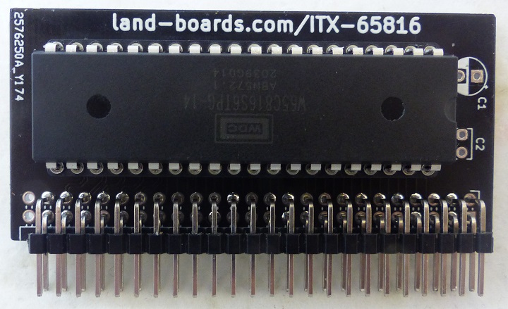
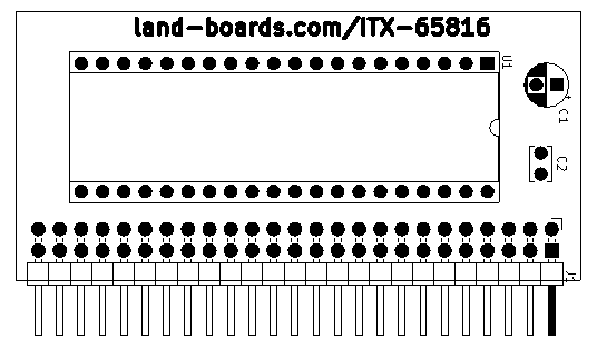
- W65C816 CPU
- 3.3V
- Running at 8.33 MHz
- Native mode (65C816 extended code) and emulation mode (65C02 code)
- Native mode allows for 24-bit address space
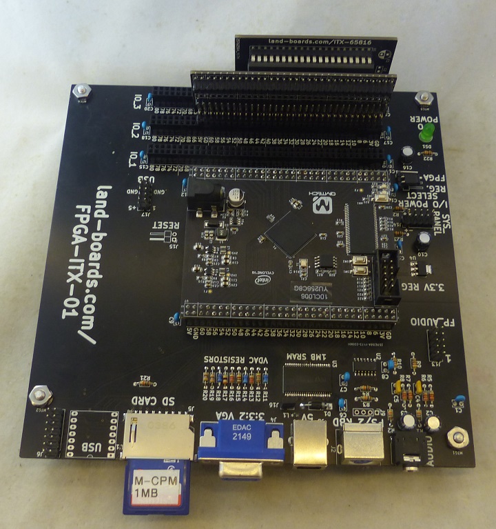
- Installs into FPGA-ITX-01 backplane
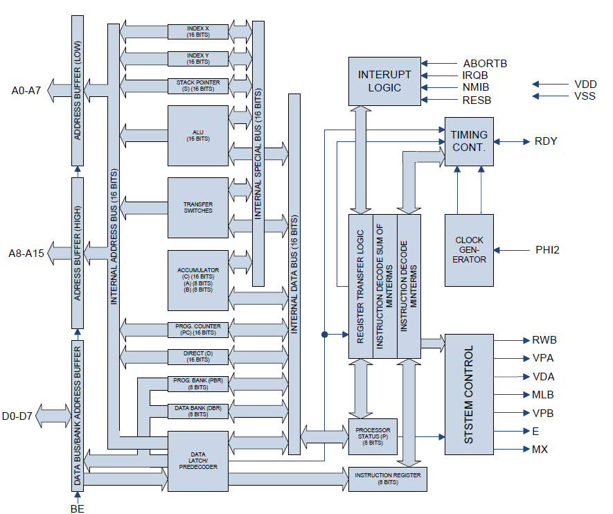
CPU Internal Block Diagram

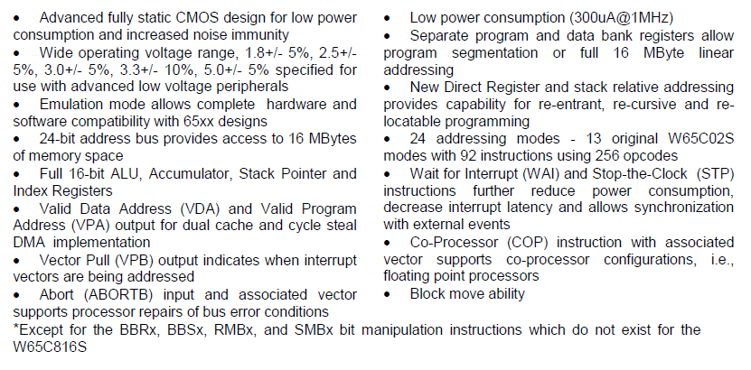
CPU Features

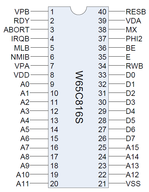
CPU Pinout

NOP Generator
- Validate connections between CPU and FPGA
- Address line count up
- Data lines send out NOP ($EA) opcode controlled by RWB and CPU Clock
- Control lines
- Clock to CPU (from clock divider)
- RWB from CPU
- Bus control lines
- VHDL code
  -- CPU signals
  IO_CPU_DATA <= x"EA" when i_CPU_RWB = '1' else
    (others => 'Z');

  CPUClkGen : entity work.counter
    generic map (n => 20)
    port map (
      clock	=> w_cpuClk,
      clear	=> '0',
      count	=> '1',
      Q		=> w_CPUClkCount
    );

  process (i_clk_50)
    begin
      if rising_edge(i_clk_50) then
        o_CPU_PHI2 <= w_CPUClkCount(4);
      end if;
    end process;

  o_CPU_RESB_n <= i_n_reset;

  o_CPU_IRQB_n	<= '1';
  o_CPU_NMIB_n	<= '1';
  o_CPU_ABORTB	<= '1';
  o_CPU_BE			<= '1';
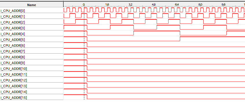
- Used scope and observed Address lines count up
- SignalTap capture of address lines at 0xFFFF to 0x0000 transition

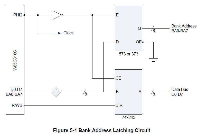
Upper address bits latch

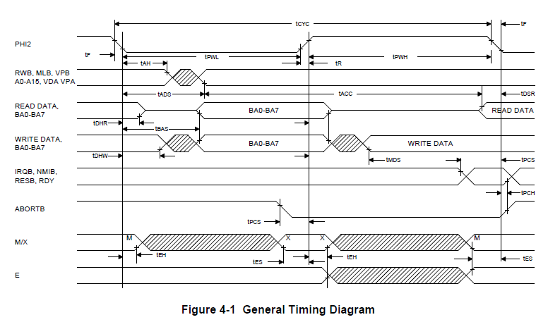
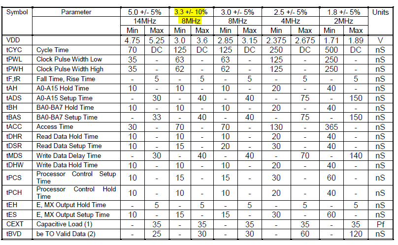
Timing


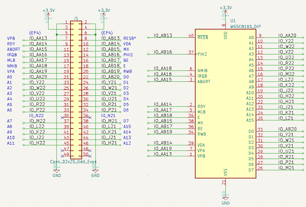
Connectors

Schematics

Pin List
| U8 PIN
|
EP4CE15/55
|
5CEFA2
|
10C1006
|
FUNCTION
|
|
U8 PIN
|
EP4CE15/55
|
5CEFA2
|
10C1006
|
FUNCTION
|
| 1
|
GND
|
GND
|
GND
|
GND
|
|
2
|
GND
|
GND
|
GND
|
GND
|
| 3
|
3.3V
|
3.3V
|
3.3V
|
3.3V
|
|
4
|
3.3V
|
3.3V
|
3.3V
|
3.3V
|
| 5
|
GND
|
GND
|
GND
|
GND
|
|
6
|
GND
|
GND
|
GND
|
GND
|
| 7
|
PIN_AA13
|
PIN_AA14
|
PIN_R9
|
CPU_VPB
|
|
8
|
PIN_AB13
|
PIN_AA13
|
PIN_T9
|
CPU_RESB*
|
| 9
|
PIN_AA14
|
PIN_AA15
|
PIN_R10
|
CPU_RDY
|
|
10
|
PIN_AB14
|
PIN_AB15
|
PIN_T10
|
CPU_VDA
|
| 11
|
PIN_AA15
|
PIN_Y15
|
PIN_R11
|
CPU_ABORT
|
|
12
|
PIN_AB15
|
PIN_Y14
|
PIN_T11
|
CPU_MX
|
| 13
|
PIN_AA16
|
PIN_AB18
|
PIN_R12
|
CPU_IRQB
|
|
14
|
PIN_AB16
|
PIN_AB17
|
PIN_T12
|
CPU_PHI2
|
| 15
|
PIN_AA17
|
PIN_Y17
|
PIN_N9
|
CPU_MLB
|
|
16
|
PIN_AB17
|
PIN_Y16
|
PIN_M9
|
CPU_BE
|
| 17
|
PIN_AA18
|
PIN_AA18
|
PIN_M10
|
CPU_NMIB
|
|
18
|
PIN_AB18
|
PIN_AA17
|
PIN_P9
|
CPU_E
|
| 19
|
PIN_AA19
|
PIN_AA20
|
PIN_P11
|
CPU_VPA
|
|
20
|
PIN_AB19
|
PIN_AA19
|
PIN_N11
|
CPU_RWB
|
| 21
|
PIN_AA20
|
PIN_Y20
|
PIN_R13
|
CPU_A0
|
|
22
|
PIN_AB20
|
PIN_Y19
|
PIN_T13
|
CPU_D0
|
| 23
|
PIN_Y22
|
PIN_AB21
|
PIN_T15
|
CPU_A1
|
|
24
|
PIN_Y21
|
PIN_AB20
|
PIN_T14
|
CPU_D1
|
| 25
|
PIN_W22
|
PIN_AA22
|
PIN_N12
|
CPU_A2
|
|
26
|
PIN_W21
|
PIN_AB22
|
PIN_M11
|
CPU_D2
|
| 27
|
PIN_V22
|
PIN_W22
|
PIN_R14
|
CPU_A3
|
|
28
|
PIN_V21
|
PIN_Y22
|
PIN_N13
|
CPU_D3
|
| 29
|
PIN_U22
|
PIN_Y21
|
PIN_N14
|
CPU_A4
|
|
30
|
PIN_U21
|
PIN_W21
|
PIN_P14
|
CPU_D4
|
| 31
|
PIN_R22
|
PIN_U22
|
PIN_P16
|
CPU_A5
|
|
32
|
PIN_R21
|
PIN_V21
|
PIN_R16
|
CPU_D5
|
| 33
|
PIN_P22
|
PIN_V20
|
PIN_N16
|
CPU_A6
|
|
34
|
PIN_P21
|
PIN_W19
|
PIN_N15
|
CPU_D6
|
| 35
|
PIN_N22
|
PIN_U21
|
PIN_M16
|
N/C
|
|
36
|
PIN_N21
|
PIN_U20
|
PIN_M15
|
N/C
|
| 37
|
PIN_M22
|
PIN_R22
|
PIN_L16
|
CPU_A7
|
|
38
|
PIN_M21
|
PIN_T22
|
PIN_L15
|
CPU_D7
|
| 39
|
PIN_L22
|
PIN_P22
|
PIN_P15
|
CPU_A8
|
|
40
|
PIN_L21
|
PIN_R21
|
PIN_M12
|
CPU_A15
|
| 41
|
PIN_K22
|
PIN_T20
|
PIN_L14
|
CPU_A9
|
|
42
|
PIN_K21
|
PIN_T19
|
PIN_L13
|
CPU_A14
|
| 43
|
PIN_J22
|
PIN_P16
|
PIN_K16
|
CPU_A10
|
|
44
|
PIN_J21
|
PIN_P17
|
PIN_K15
|
CPU_A13
|
| 45
|
PIN_H22
|
PIN_N20
|
PIN_K12
|
CPU_A11
|
|
46
|
PIN_H21
|
PIN_N21
|
PIN_J12
|
CPU_A12
|
| 47
|
N/C
|
N/C
|
N/C
|
N/C
|
|
48
|
N/C
|
N/C
|
N/C
|
N/C
|
| 49
|
N/C
|
N/C
|
N/C
|
N/C
|
|
50
|
N/C
|
N/C
|
N/C
|
N/C
|
MultiComp Build
- GitHub repo
- 24-bit address (upper 8-bits latched in FPGA)
- 8.33 MHz operation
- Tested/Working
- Running OSI 6502
- Microsoft 8K BASIC "in ROM"
- VGA output
- 1MB SRAM
- PS/2 Keyboard
Resources
Installed

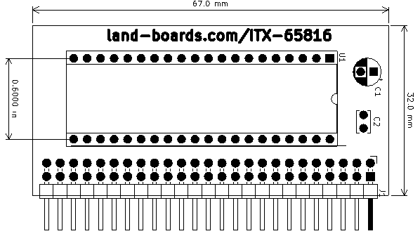
Mechanicals

Assembly Sheet
