ER-CVPOTS4
Revision as of 17:50, 18 January 2023 by Blwikiadmin (talk | contribs)
Contents
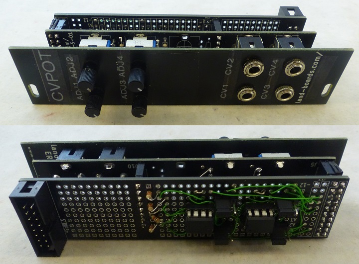
Features
- Pot controlled CV generator
- Useful for testing VCOs, etc
- (4) Buffered CV Outputs
- 4 Pots
- RV1-RV4 used
- RV5, RV6 not used
- 4 Jacks
- RV1 controls J1, etc
- Output voltage Levels are assignable via jumpers
- +5V/GND
- +12V/-12V
- +12V/GND
Opamp Choices
- 8 pin Opamps
Schematic
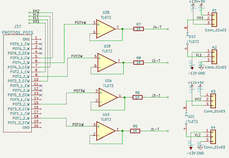
Opamp buffers
- CV Voltage selection headers
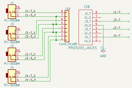
Output jacks
- Jack grounds connected on Controls card (3 jumpers)
- Single ground connection on daughtercard (1 jumper)
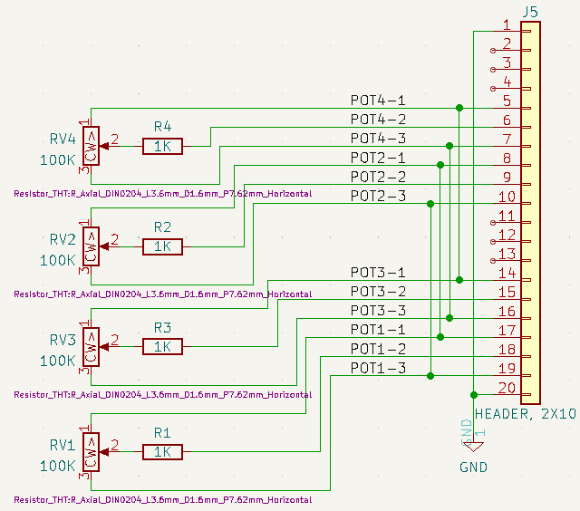
Pots on Controls card
- Connections of CW and CCW
- RV1 goes to RV2
- RV3 goes to RV4
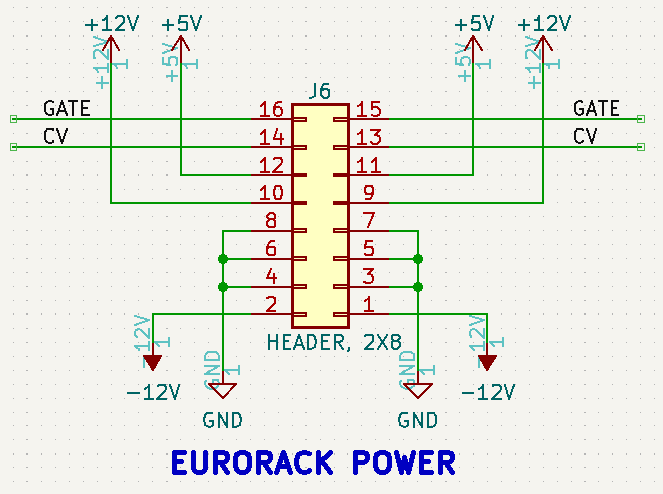
J6 - Eurorack Power
- J6 on the I/O card
- Eurorack power
- 2x5 IDC
- GATE, CV not connected
Control Board Wiring
- NODE: GND, J1-GND to J3-GND
- NODE: GND, J2-GND to J4-GND
- NODE: GND, J3-GND to J4-GND
- NODE: GND, RV1-3 to RV3-3
- NODE: GND, RV2-3 to RV4-3
- NODE: VCC, RV1-1 to RV3-1
- NODE: VCC, RV2-1 to RV4-1
Daughtercard wiring
- NODE: J1-T*, U1-1 to R5 (other side goes to J38-8)
- NODE: J2-T*, U1-7 to R8 (other side goes to J38-4)
- NODE: J3-T*, U2-1 to R6 (other side goes to J38-6)
- NODE: J4-T*, U2-7 to R7 (other side goes to J38-2)
- NODE: LB1, U1-1 to U1-2
- NODE: LB2, U1-6 to U1-7
- NODE: LB3, U2-1 to U2-2
- NODE: LB4, U2-6 to U2-7
- NODE: GND, J38-3 or 5 (nearest GND) bus hole
- NODE: VH1, H1-2 (+12/+5 header) to U1-8
- NODE: VL1, H2-2 (GND header) to U1-4
- NODE: VH2, H3-2 (+12/+5 header) to U2-8
- NODE: VL2, H4-2 (GND header) to U2-4
- NODE: VH1, U1-8 to J37-8 (POT2-CW)
- NODE: VL1, U1-4 to J37-10 (POT2-10)
- NODE: VH2, U2-8 to J37-5 (POT4-CW)
- NODE: VL2, U2-4 to J37-7 (POT4-CCW
- NODE: POT1W, J37-18 to U1-3
- NODE: POT2W, J37-9 to U1-5
- NODE: POT3W, J37-15 to U2-3
- NODE: POT4W, J37-6 to U2-5
Parts Lists
Daughtercard Parts List
| Find | Qty | Ref Des | Part Number |
|---|---|---|---|
| 1 | 4 | H1-H4 | Conn_01x03 |
| 2 | 1 | J5 | HEADER, 2X10 |
| 3 | 1 | J6 | HEADER, 2X8 |
| 4 | 1 | J10 | Conn_01x08 |
| 5 | 4 | R5-R8 | 1K |
| 10 | 2 | R6, R7 | 1K |
| 6 | 2 | U1, U2 | SOCKET, 8 PIN |
| 7 | 2 | U1, U2 | TL072 |
Controls card Parts List
- RV1-RV4 = B100K pots
- R1-R4 = 1K
- J1-J4 = PJ301BM
- J5 = Socket, Female, 2x10
- J10 = Socket, Female, 1x8
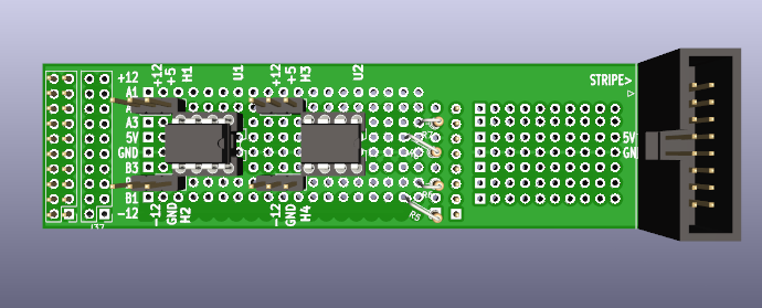
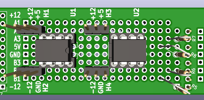
3D PCB Layout
- Board soldermask is actually black, but shown in green for contrast
- Details
