Features
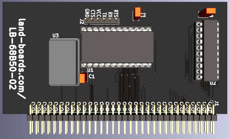
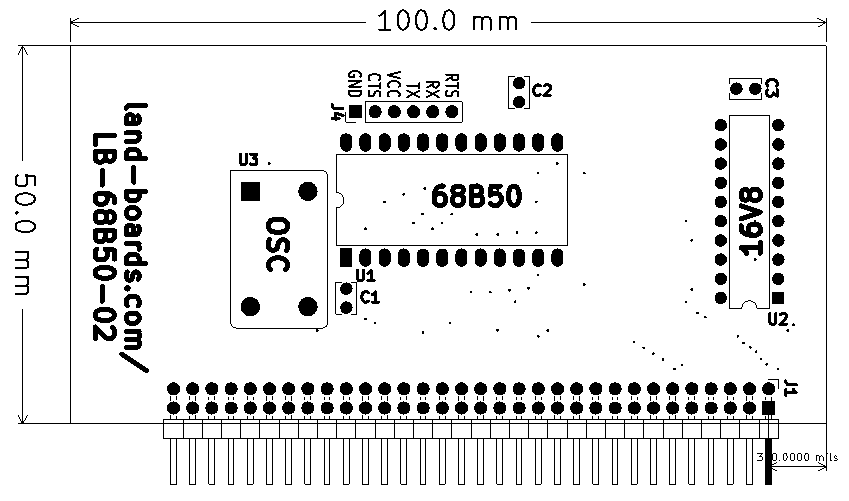
- Serial/Parallel I/O Card
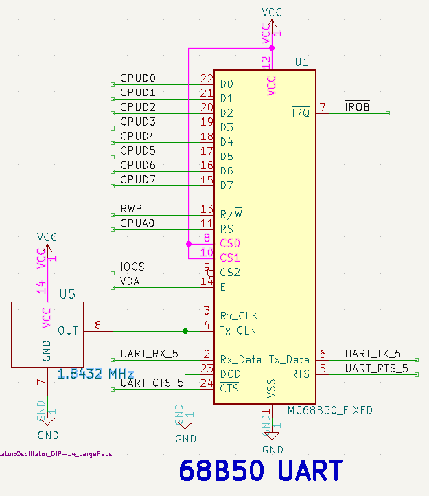
- 68B50 UART
- 1.8432 MHz oscillator
- Baud Rate Clock (115,200 baud oscillator)
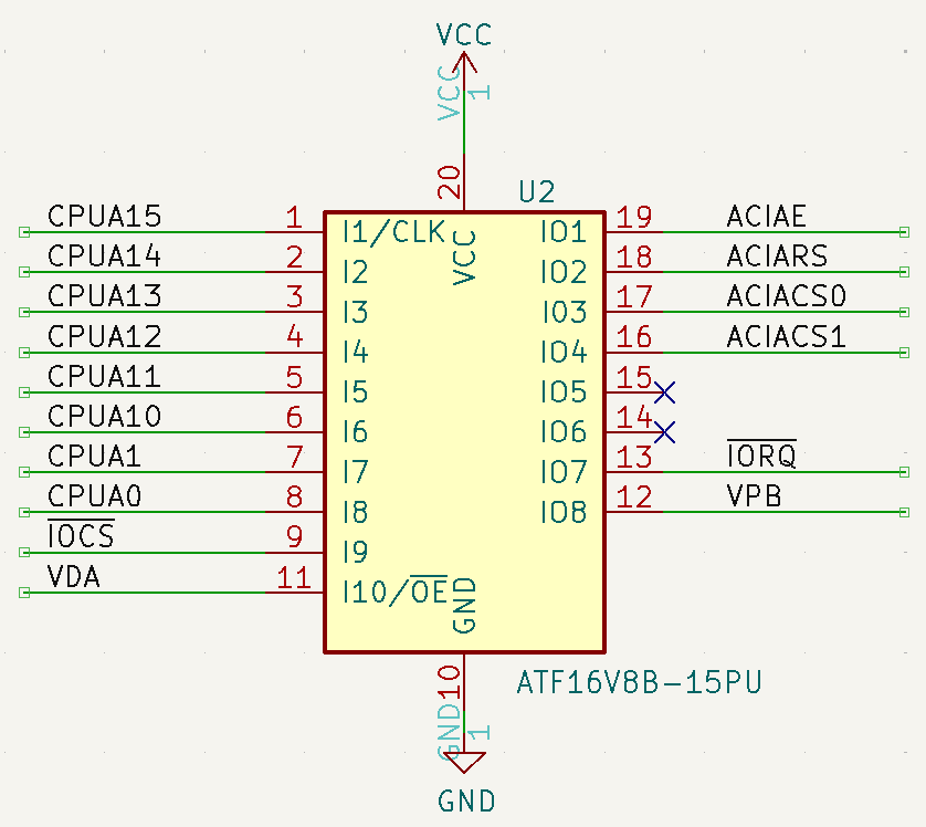
- Control PLD
- 100x50mm card
Design
ACIA
- 68B50 UART
- Baud Rate Clock (115,200 baud oscillator)

PLD

LB-68B50-02_65CXX_PLD PLD Listing
Name       LB-68B50-02_65CXX_PLD;
Partno     ATF16V8B;
Date       08/19/24;
Revision   01;
Designer   DOUG G;
Company    LAND BOARDS LLC;
Assembly   LB-68B50-02_65CXX_U2;
Location   Rustbelt, US;
Device     G16V8;

/*
	68B50 Control for LB-65CXX-01 CPU board
	VDA is PH2OUT
	PH2OUT high during read/write cycles
	0x8000-0x8FFF - 4KB I/O space
*/

/* Control inputs */
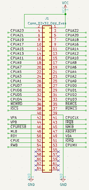
PIN    1   = CPUA15;
PIN    2   = CPUA14;
PIN    3   = CPUA13;
PIN    4   = CPUA12;
PIN    5   = CPUA11;
PIN    6   = CPUA10;
PIN    7   = CPUA1;
PIN    8   = CPUA0;
PIN    9   = !IOCS;
PIN    11   = VDA;
PIN    12   = VPB;
PIN    14   = !IORQ;

/* Address Decode and Chip Select outputs */
PIN    16  = ACIACS1;
PIN    17  = ACIACS0;
PIN    18  = ACIARS;
PIN    19  = ACIAE;

ACIACS1 = CPUA15 & !CPUA14 & !CPUA13 & !CPUA12 & IOCS & VPB;

ACIACS0 = CPUA15 & !CPUA14 & !CPUA13 & !CPUA12 & IOCS & VPB;

ACIARS = CPUA0;

ACIAE = CPUA15 & !CPUA14 & !CPUA13 & !CPUA12 & IOCS & VPB;
LB-68B50-02_Z80_PLD PLD Listing
Name       LB-68B50-02_PLD;
Partno     ATF16V8B;
Date       08/19/24;
Revision   01;
Designer   DOUG G;
Company    LAND BOARDS LLC;
Assembly   LB-685-02_U2;
Location   Rustbelt, US;
Device     G16V8;

/*
	68B50 Control for Z80 CPU board
*/

/* Control inputs */
PIN    1   = CPUA15;
PIN    2   = CPUA14;
PIN    3   = CPUA13;
PIN    4   = CPUA12;
PIN    5   = CPUA11;
PIN    6   = CPUA10;
PIN    7   = CPUA1;
PIN    8   = CPUA0;
PIN    9   = !IOCS;
PIN    11   = VDA;
PIN    12   = VPB;
PIN    14   = !IORQ;

/* Address Decode and Chip Select outputs */
PIN    16  = ACIACS1;
PIN    17  = ACIACS0;
PIN    18  = ACIARS;
PIN    19  = ACIAE;

ACIACS1 = !CPUA1 & IOCS & IORQ;

ACIACS0 = !CPUA1 & IOCS & IORQ;

ACIARS = CPUA0;

ACIAE = !CPUA1 & IOCS & IORQ;
LB-68B50-02_68XX_PLD PLD Listing
Name       LB-68B50-02_68XX_PLD;
Partno     ATF16V8B;
Date       08/25/24;
Revision   01;
Designer   DOUG G;
Company    LAND BOARDS LLC;
Assembly   LB-68B50-02_68XX_U2;
Location   Rustbelt, US;
Device     G16V8;

/*
	68B50 Control for LB-6809-01 and LB-6802-01 CPU boards
	VDA is PH2OUT
	PH2OUT high during read/write cycles
	0x8000-0x8FFF - 4KB I/O space
*/

/* Control inputs */
PIN    1   = CPUA15;
PIN    2   = CPUA14;
PIN    3   = CPUA13;
PIN    4   = CPUA12;
PIN    5   = CPUA11;
PIN    6   = CPUA10;
PIN    7   = CPUA1;
PIN    8   = CPUA0;
PIN    9   = !IOCS;		/* IOCS is IO space decoded on all CPU cards */
PIN    11   = VDA;		/* VDA is PH2OUT is enable on 65CXX CPU */
PIN    12   = VPB;		/* VPB is enable on 6802 and 6809 CPUs	*/
PIN    14   = !IORQ;	/* IORQ* is enable on Z80 cards			*/

/* Address Decode and Chip Select outputs */
PIN    16  = ACIACS1;
PIN    17  = ACIACS0;
PIN    18  = ACIARS;
PIN    19  = ACIAE;

ACIACS1 = CPUA15 & !CPUA14 & !CPUA13 & !CPUA12 & IOCS & VPB;

ACIACS0 = CPUA15 & !CPUA14 & !CPUA13 & !CPUA12 & IOCS & VPB;

ACIARS = CPUA0;

ACIAE = CPUA15 & !CPUA14 & !CPUA13 & !CPUA12 & IOCS & VPB;

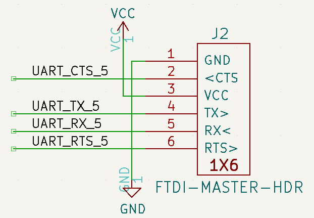
- GND
- CTS (in)
- VCC
- TX (out)
- RX (in)
- RTS (out)
Backplane

Mechanicals
Rev 1

Checkout
Rev 1

Assembly Sheet
