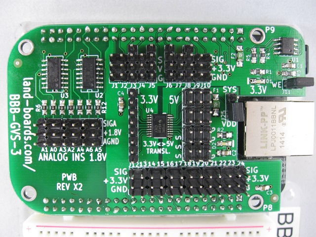
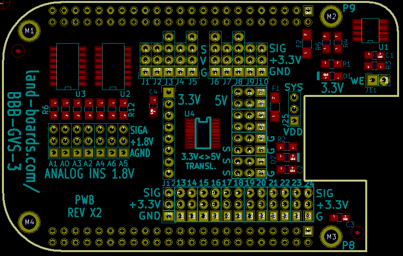
BBB-GVS-3
Features
- (19) GPIOs, GVS pins
- GVS pins
- (3) UARTs, GVTxRx pins
- GVTxRx pins
- (1) I2C bus, GVSdaSck
- GVSdaSck
- (8) Channels of 3.3V to 5V level translators
- Use female to female jumpers to route the GPIO lines to the translator channels
- 5V side has GVS pins
- (7) 1.8V analog GVS connections with analog voltage/ground
- Buffer opamps on the analog inputs
- 5V pins are all ESD protected pins with 15 kV of protection
- Selectable 5V source (SYS_5V or VDD_5V)
LEDs for 3.3V and 5V power
- Cape configuration EEPROM with write enable jumper
- Beaglebone Black form factor
Connectors
Card Header	GPIO	BBB Pin
J1	SPI1_D1	P9_30
J2	GPIO3_19	P9_27
J3_3	UART1_RX	P9_26
J3_4	UART1_TX	P9_24
J4	GPIO1_17	P9_23
J5_3	UART2_TX	P9_21
J5_4	UART2_RX	P9_22
J6_3	I2C1_SDA	P9_18
J6_4	I2C1_SCL	P9_17
J7	GPIO1_16	P9_15
J8_3	UART4_TX	P9_13
J8_4	UART4_RX	P9_11
J9	EHRPWM1A	P9_14
J10	GPIO1_28	P9_12
J12	GPIO1_29	P8_26
J13	EHRPWM2A	P8_19
J14	GPIO2_1	P8_18
J15	GPIO0_27	P8_17
J16	GPIO1_14	P8_16
J17	GPIO1_15	P8_15
J18	EHRPWM2B	P8_13
J19	GPIO1_12	P8_12
J20	GPIO1_13	P8_11
J21	TIMER5	P8_09
J22	TIMER6	P8_10
J23	TIMER4	P8_07
J24	TIMER7	P8_08
EEPROM Connections
- The EEPROM connections are on I2C and have on-board pullup resistors.
- The connections are local to the card.
- The EEPROM part number is CAT24C256WI-GT3 [1]
J11 - WE
- GND
- VCC
- WE


