Difference between revisions of "ER-PROTO-01"
Jump to navigation
Jump to search
Blwikiadmin (talk | contribs) |
Blwikiadmin (talk | contribs) |
||
| (22 intermediate revisions by the same user not shown) | |||
| Line 1: | Line 1: | ||
| + | [[File:tindie-mediums.png|link=https://www.tindie.com/products/28599/]] | ||
| + | |||
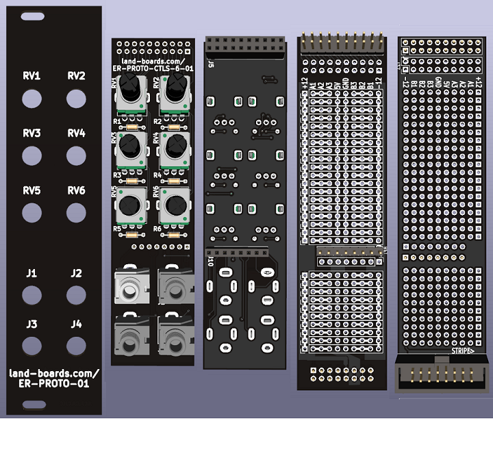
[[FILE:ER-PROTO-PANEL-01-SET_FRONT_REAR-3D-720px.png]] | [[FILE:ER-PROTO-PANEL-01-SET_FRONT_REAR-3D-720px.png]] | ||
| Line 89: | Line 91: | ||
=== Arduino NANO MOZZI === | === Arduino NANO MOZZI === | ||
| − | + | [[Arduino NANO MOZZI on ER-PROTO-01]] | |
| − | |||
| − | [[ | ||
| − | |||
| − | |||
| − | [[ | + | [[file:ER-PROTO-01-NANO-MOZZI_P1080687-720PX.jpg]] |
| − | + | [[file:ER-PROTO-01-NANO-MOZZI_P1080693-720PX.jpg]] | |
| − | |||
| − | |||
| − | |||
| − | |||
| − | |||
| − | |||
| − | |||
| − | |||
| − | |||
| − | |||
| − | |||
| − | |||
| − | |||
| − | |||
| − | |||
| − | |||
| − | [[ | ||
| − | |||
| − | |||
| − | |||
| − | |||
| − | |||
| − | |||
| − | |||
| − | |||
| − | |||
| − | |||
| − | |||
| − | |||
| − | |||
| − | |||
| − | |||
| − | |||
| − | |||
| − | |||
| − | |||
| − | |||
| − | |||
| − | |||
| − | |||
| − | |||
| − | |||
| − | |||
| − | |||
| − | |||
| − | |||
| − | |||
| − | |||
| − | |||
| − | |||
| − | |||
| − | |||
| − | |||
| − | |||
| − | |||
| − | |||
| − | |||
| − | |||
| − | |||
| − | |||
| − | |||
| − | |||
| − | |||
| − | |||
| − | |||
| − | |||
| − | |||
| − | |||
| − | |||
| − | |||
| − | |||
| − | |||
| − | |||
| − | |||
| − | |||
| − | |||
| − | |||
| − | |||
| − | |||
| − | |||
| − | |||
| − | |||
| − | |||
| − | |||
| − | |||
| − | |||
| − | |||
| − | |||
| − | |||
| − | |||
| − | |||
| − | |||
| − | |||
| − | |||
| − | |||
| − | |||
| − | |||
| − | |||
| − | |||
| − | |||
| − | |||
| − | |||
| − | |||
| − | |||
| − | |||
| − | |||
| − | |||
| − | |||
| − | |||
| − | |||
| − | |||
| − | |||
| − | |||
| − | |||
| − | |||
| − | |||
| − | |||
| − | |||
| − | |||
| − | |||
| − | |||
| − | |||
| − | |||
| − | |||
| − | |||
| − | |||
| − | |||
| − | |||
| − | |||
| − | |||
| − | |||
| − | |||
| − | |||
| − | |||
| − | |||
| − | |||
| − | |||
| − | |||
| − | |||
| − | |||
| − | |||
| − | |||
=== CV4 - 4 Control Voltages === | === CV4 - 4 Control Voltages === | ||
| − | + | [[ER-CVPOTS4]] | |
| − | |||
| − | |||
| − | |||
| − | |||
| − | |||
| − | |||
| − | |||
| − | |||
| − | |||
| − | |||
| − | |||
| − | |||
| − | |||
| − | |||
| − | |||
| − | |||
| − | |||
| − | |||
| − | |||
| − | |||
| − | |||
| − | |||
| − | |||
| − | |||
| − | |||
| − | |||
| − | |||
| − | |||
| − | |||
| − | |||
| − | |||
| − | |||
| − | |||
| − | |||
| − | |||
| − | |||
| − | |||
| − | |||
| − | |||
| − | |||
| − | |||
| − | |||
| − | |||
| − | |||
| − | |||
| − | |||
| − | |||
| − | |||
| − | |||
| − | |||
| − | |||
| − | |||
| − | [[ | ||
| − | |||
| − | |||
| − | |||
| − | |||
| − | |||
| − | |||
| − | |||
| − | |||
| − | |||
| − | |||
| − | |||
| − | |||
| − | + | [[file:ER-PROTO-01-CV4_P1090031-F_B_720px.jpg]] | |
| − | |||
| − | |||
| − | |||
| − | |||
| − | |||
| − | |||
| − | |||
| − | |||
| − | |||
| − | |||
| − | |||
| − | |||
| − | |||
| − | |||
| − | |||
| − | |||
| − | |||
| − | |||
| − | |||
| − | |||
| − | === | + | === Noise Generator === |
| − | + | [[Noise_Generator_on_ER-PROTO-01|Noise Generator on ER-PROTO-01]] | |
| − | |||
| − | |||
| − | |||
| − | |||
| − | |||
| − | |||
| − | |||
| − | |||
| − | |||
| − | |- | ||
| − | |||
| − | |||
| − | |||
| − | |||
| − | |||
| − | |||
| − | |||
| − | |||
| − | |||
| − | |||
| − | |||
| − | |||
| − | |||
| − | |||
| − | |||
| − | |||
| − | |||
| − | |||
| − | |||
| − | |||
| − | |||
| − | |||
| − | |||
| − | |||
| − | |||
| − | |||
| − | |||
| − | |||
| − | |||
| − | |||
| − | |||
| − | |||
| − | |||
| − | |||
| − | |||
| − | |||
| − | + | [[file:ER-PROTO-01_NOISE_P1080751-720px.jpg]] | |
| − | + | [[file:ER-PROTO-01_NOISE_P1080755-720px.jpg]] | |
| − | |||
| − | |||
| − | |||
| − | |||
=== Slew Rate Controller === | === Slew Rate Controller === | ||
| − | + | [[Slew Rate Controller on ER-PROTO-01]] | |
| − | |||
| − | |||
| − | |||
| − | |||
| − | |||
| − | |||
| − | + | == Assembly Sheet == | |
| − | |||
| − | |||
| − | |||
| − | [ | + | * [[ER-PROTO-01 Assembly Sheet]] |
Latest revision as of 17:48, 18 January 2023
Features
- Eurorack Prototyping card set
- 6 HP wide (30mm) front panel
- 3U tall
- Three card set
- Board interconnect headers duplicated on headers
- 30mm wide front panel
- 28mm wide panel and daughtercards
- 6 POTS
- Marked as RV1-RV5
- Series resistors on pot wiper
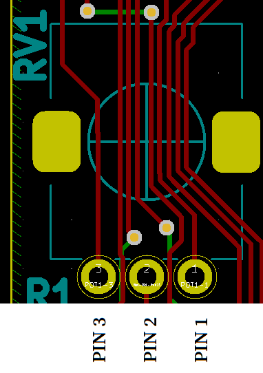
- All 3 pot pins brought to top header
- 4 Jacks
- Marked as J1-J4
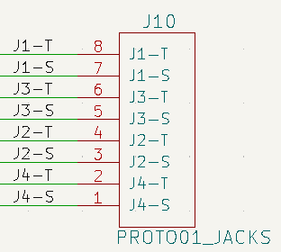
- Tip/sleeve brought to header near middle/bottom
- Pots on top, jacks on bottom of card
- Easier to adjust pots without bumping into pots
- Pots more often accessed than jacks
- Large prototyping area
- 58 nodes with 3 holes per node (29 per "side")
- +12V, -12V down board edges
- 5V/GND down center of card
- Bussed connections horizontally
- Front Panel with generic labels
- Cover with White on Black P-Touch labels
Connectors
- J1-J4 are front panel connectors
Inter-card Connectors
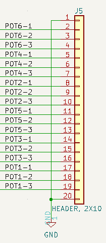
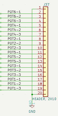
Pots
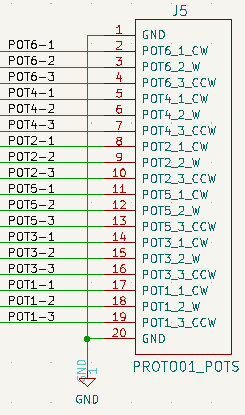
- J5 on the Controls card and J5 on the I/O card
- Pot connections
- POTx-1 is fully CW connects to wiper
- POTx-2 is wiper
- POTX-3 is fully CCW connects to wiper
- To make pot into voltage control
- POTx-1 (CW) = +5V
- POTx-13CCW = GND
- Wire RV1-1 to RV3-1 to RV5-1 on controls card
- Wire RV1-3 to RV3-3 to RV5-3 on controls card
- Wire RV2-1 to RV4-1 to RV6-1 on controls card
- Wire RV2-3 to RV4-3 to RV6-3 on controls card
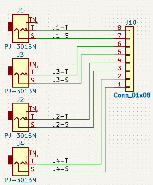
Jacks
- J6 on the controls card and J37 on the I/O card
Daughtercard Connectors
J5, J37 - POT connectione
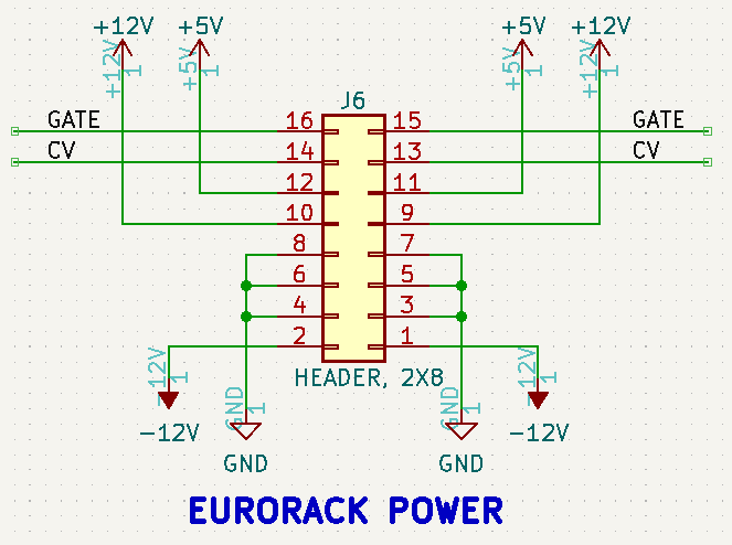
J6 - Eurorack Power
- J6 on the I/O card
- Eurorack power
- 2x5 IDC
- GATE, CV not connected
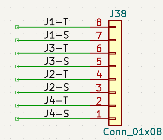
J10 - Jacks connections on Controls card
J38 - Jacks connections
Examples
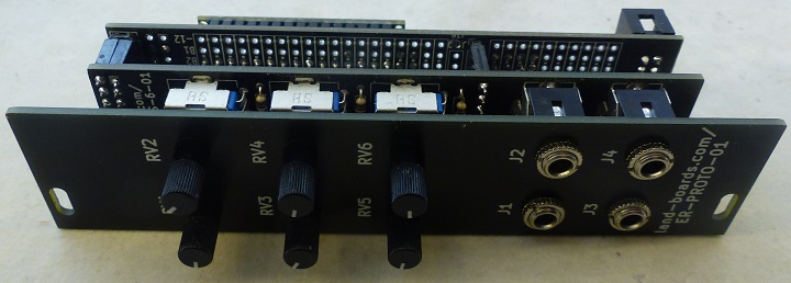
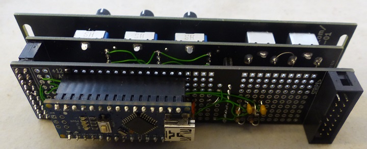
Arduino NANO MOZZI
Arduino NANO MOZZI on ER-PROTO-01
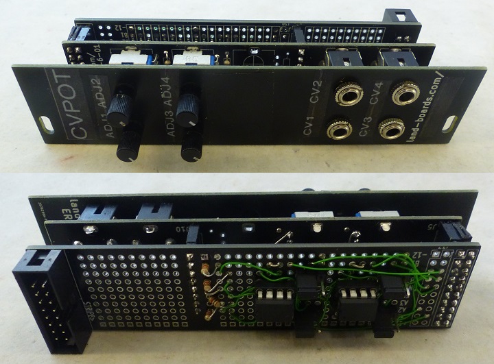
CV4 - 4 Control Voltages
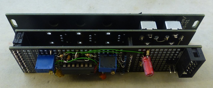
Noise Generator
Noise Generator on ER-PROTO-01
Slew Rate Controller
Slew Rate Controller on ER-PROTO-01

