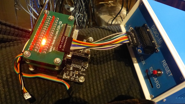
IOP16 General Purpose I/O (GPIO)
Jump to navigation
Jump to search
General-purpose I/O
From Neal Crook's simple GPIO unit.
- A simple GPIO unit for a 6809 multicomp.
- Aims to provide a number of programmable I/O lines all accessed through an indirect mechanism using 2 locations in the processor address space.
- The operation is fully synchronous on the master clock; a clock enable determines when the state changes.
- Design by Neal Crook foofoobedoo@gmail.com Jun2015.
- You are free to use this file in your own projects but must never charge for it nor use it without acknowledgement.
GPIO PROGRAMMING INTERFACE
- The software interface is through 2 read/write registers, usually decoded at the following addresses :
- regSel = 0 - GPIOADR
- regSel = 1 - GPIODAT
- GPIOADR specifies the register to access. GPIODAT provides data read/write to selected register.
- Using a 16-bit store you can generate an atomic register select/data write.
- There is no equivalent mechanism for reads.
- Therefore, if any ISR ever accesses a GPIO register, you must bracket any GPIO register operations with disable/enable of interrupts.
- It's probably safest simply to never access GPIO within an ISR.
- When you have written a value to GPIOADR (either with an 8-bit or 16-bit store) you can perform multiple GPIODAT reads and writes to the selected register; there is no need to re-write GPIOADR until you wish to select a different register. Beware of interrupts though; see note above.
- For each group of physical pins there are 2 registers in GPIO.
- The odd register is the data direction register
- The even register is the data register.
- A 0 in the data direction register marks the bit as an output, and a 1 marks it as an input
- (mnemonic: 0utput, 1nput)
- A write to the data register sends the write data to the pin for each bit that is an output
- A read from the data register samples the pin for each bit that is an input, and returns the last value written for each bit that is an output.
- When you switch a pin from input to output, it will immediately assume the value that was most recently written to it.
- The following registers are implemented:
- 0 DAT0 bits [2:0]
- 1 DDR1 bits [2:0]
- 2 DAT2 bits [7:0]
- 3 DDR3 bits [7:0]
- After reset, GPIOADR=0, all DDR*=0 (output) all DAT*=0 (output low).
Entity
-- ____________________________________________________________________________________
-- GPIO Unit by Neal Crook - Built for 6809 Multicomp
-- https://github.com/nealcrook/multicomp6809/blob/master/multicomp/Components/GPIO/gpio.vhd
gpio : entity WORK.gpio
port MAP (
  n_reset   => w_resetClean_n,
  clk       => i_clock,
  hold      => '0',
  -- conditioned with chip select externally
  n_wr      => not w_peripWr,
  dataIn    => w_peripDataFromCPU,
  dataOut   => w_GPIO_Out,
  -- 0 for GPIOADR, 1 for GPIODAT
  regAddr   => w_peripAddr(0),
  -- GPIO
  dat0_i    => w_dat0_i,
  dat0_o    => w_dat0_o,
  n_dat0_oe => w_n_dat0_oe,
  dat2_i    => w_dat2_i,
  dat2_o    => w_dat2_o,
  n_dat2_oe => w_n_dat2_oe
);
Resources (EP4CE15)
- Logic Cells: 40
- Registers: 30
- Memory bits: 0
