Difference between revisions of "OPTOUSB"
Jump to navigation
Jump to search
Blwikiadmin (talk | contribs) |
Blwikiadmin (talk | contribs) |
||
| (112 intermediate revisions by the same user not shown) | |||
| Line 31: | Line 31: | ||
== Separate Power Domains == | == Separate Power Domains == | ||
| − | The OPTOUSB card has two distinct power domains. | + | * The OPTOUSB card has two distinct power domains. |
| − | One of the domains is the USB side where the power comes from the USB connector/cable. | + | ** One of the domains is the USB side where the power comes from the USB connector/cable. |
| − | The other power domain is on the TTL side where the power comes from the FTDI connector. | + | ** The other power domain is on the TTL side where the power comes from the FTDI connector. |
| − | This is unlike "normal" FTDI interfaces where the USB connection can power the FTDI side. | + | * This is unlike "normal" FTDI interfaces where the USB connection can power the FTDI side. |
| − | This is the purpose of the optical isolation - to isolate the ground of the USB side from the target (FTDI) side. | + | ** This is the purpose of the optical isolation - to isolate the ground of the USB side from the target (FTDI) side. |
| − | |||
| − | |||
| − | |||
| − | |||
| − | |||
| − | |||
| − | |||
| − | |||
| − | |||
| − | |||
| − | |||
| − | |||
| − | |||
| − | |||
| − | |||
| − | |||
| − | |||
| − | |||
| − | |||
| − | |||
| − | + | == Connectors == | |
| − | |||
| − | |||
| − | |||
| − | + | === J1 - Mini USB Connector === | |
| − | + | ||
| − | 5V Power | + | * Standard USB Mini connector |
| − | + | ||
| − | + | === J2 - Transmit/Receive LED connections === | |
| − | + | ||
| − | + | # PUP0 - LED Pullup to USB Power | |
| − | + | # TXLED - Transmit LED | |
| − | Run puTTY | + | # PUP1 - LED Pullup to USB Power |
| − | + | # RXLED - Receive LED | |
| − | + | ||
| − | + | === J3 - FTDI Connector === | |
| − | Rework - Rev X1 PWBs | + | |
| − | + | * Signals are references to external system | |
| + | |||
| + | # GND | ||
| + | # RTS (In to card) | ||
| + | # VCC (3.3V or 5V) - Power must be supplied to this pin | ||
| + | # Receive (Out from card) | ||
| + | # Transmit (In to card) | ||
| + | # CTS (Out from card) | ||
| + | |||
| + | == Drivers == | ||
| + | |||
| + | * [ FTDI Drivers] | ||
| + | |||
| + | == Layout == | ||
| + | |||
| + | [[File:OPTOUSB-CAD-X1.PNG]] | ||
| + | |||
| + | == Transfer Rate Characterization == | ||
| + | |||
| + | * LTSpice Simulation results | ||
| + | * 8.6uS per bit = 115,200 baud | ||
| + | |||
| + | [[File:OPTO-USB LTSpice Simulation.png]] | ||
| + | |||
| + | == Opto-Isolator Drive Circuits == | ||
| + | |||
| + | * The card has two independent, isolated power domains | ||
| + | ** The USB side is powered from the USB 5V | ||
| + | ** The FTDI side is powered from external power | ||
| + | *** Connected via header or backfeeding the FTDI connector with voltage | ||
| + | *** Voltage is one of either 3.3V or 5V | ||
| + | * [https://www.vishay.com/docs/83725/4n25.pdf 4N25 Optoisolator] used between the two sides | ||
| + | ** Optoisolator has Vf = 1.3V typical | ||
| + | ** Optoisolator has 20% CTR (min) | ||
| + | * Optoisolator can be fed with up to 50 mA of drive current | ||
| + | ** Set nominal LED drive current at half (25 mA) | ||
| + | |||
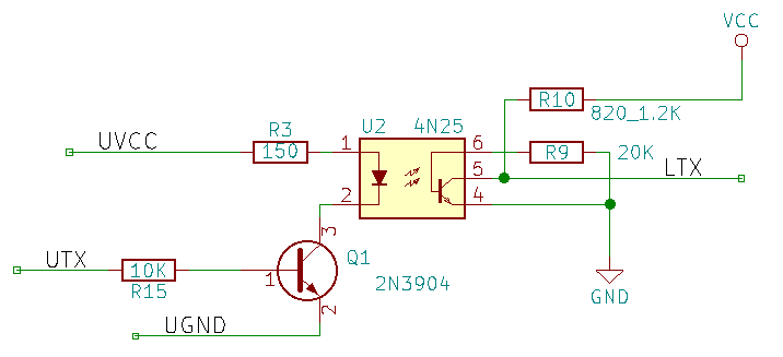
| + | === USB to FTDI Path === | ||
| + | |||
| + | [[File:USB_TO_TTL_PATH.PNG]] | ||
| + | |||
| + | ==== USB Drive Side ==== | ||
| + | |||
| + | * USB side has [https://www.mouser.com/datasheet/2/308/PZT3904_D-1814631.pdf MMBT3904] (2N3904) transistor for driving the optoisolator | ||
| + | ** Vce(Sat) at 10 mA is 0.2V | ||
| + | ** Vce(Sat) at 50 mA is 0.3V | ||
| + | * 5V drops are across transistor (0.3V), optoisolator (1.3V) and series resistor | ||
| + | ** Opto voltage is 5 - 0.3 - 1.3 = 3.4V | ||
| + | ** Opto drive current needs to be 5x the output current (due to the 20% CTR) | ||
| + | ** Assume output current (5 mA) | ||
| + | ** Optoisolator LED drive current needs to be 25 mA | ||
| + | ** 3.4V / .025A = 136 Ohms (Use 150 Ohms for drive series resistor) | ||
| + | *** 150 Ohms will be 22.6 mA drive (good compromise drive current value) | ||
| + | *** 22.6 mA drive current at 20% CTR will allow collector current to be 4.5 mA | ||
| + | * Transistor base resistor | ||
| + | ** HFE(min)=100 @Ice=10mA, HFE(min) = 60 @Ice=50mA | ||
| + | *** Use HFE=60 | ||
| + | ** 4.7V across resistor, HFE=60, Ice =25mA = 11.3K Ohm resistor | ||
| + | ** Drive with 5V, 4.7V across 10K is 0.47 mA | ||
| + | ** 0.47mA * 60 = 28.2mA (>25 mA) | ||
| + | |||
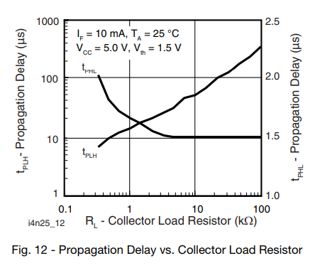
| + | ==== FTDI-Side Collector Pull-up Resistor ==== | ||
| + | |||
| + | * 25 mA into opto | ||
| + | * CTR(min) = 20% | ||
| + | * ~5mA output current | ||
| + | |||
| + | [[File:4N25 Collector resistor value cross over chart.PNG]] | ||
| + | |||
| + | * Optimal resistor value is at cross-over point where the H-L and L-H prop delays trade-off | ||
| + | ** ~1.2K | ||
| + | |||
| + | ===== 5V FTDI side Collector Pull-up Resistor ===== | ||
| + | |||
| + | * For 5V, that's about 1.2K | ||
| + | ** 5V at 1.2K ohms is 4.1 mA | ||
| + | *** 4.5 mA collector current (from above) | ||
| + | * Use 1.2K pull-up from above | ||
| + | |||
| + | ===== 3.3V FTDI side Collector Pull-up Resistor ===== | ||
| + | |||
| + | * 4N25 is not characterized for 3.3V operation in the chart but assume the same current | ||
| + | * Vce(sad) = 0.3V | ||
| + | * 3.3-0.3 = 3V | ||
| + | * 3V / 0.0041A = 731 ohms (680 or 750 are standard 5% values that are near) | ||
| + | * Use 820 ohm pull-up | ||
| + | |||
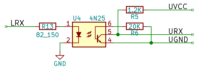
| + | === FTDI to USB Path === | ||
| + | |||
| + | * Drive FTDI side from [https://www.ti.com/lit/ds/symlink/sn74ac14.pdf?HQS=dis-mous-null-mousermode-dsf-pf-null-wwe&ts=1667128698583&ref_url=https%253A%252F%252Fwww.ti.com%252Fgeneral%252Fdocs%252Fsuppproductinfo.tsp%253FdistId%253D26%2526gotoUrl%253Dhttps%253A%252F%252Fwww.ti.com%252Flit%252Fgpn%252Fsn74ac14 74AC14] | ||
| + | ** 74AC14 outputs 24 mA Iol or Ioh | ||
| + | |||
| + | [[File:TTL_TO_USB_PATH.PNG]] | ||
| + | |||
| + | ==== 5V Drive from FTDI Side ==== | ||
| + | |||
| + | * 150 Ohm series resistor | ||
| + | ** 5V-1.3V = 3.7V | ||
| + | ** 3.7V / 150 Ohms = 24mA | ||
| + | * Could drop to 180 Ohms for better margin or double up with 2 drivers/series 300 Ohm resistors in future re-design | ||
| + | |||
| + | ==== USB Side Collector Resistor ==== | ||
| + | |||
| + | * Same as above 5V Collector resistor calculation, 1.2K ohms | ||
| + | |||
| + | ==== 3.3V Drive from FTDI Side ==== | ||
| + | |||
| + | * 82 Ohm series resistor | ||
| + | ** 3.3V-1.3V = 2.0V | ||
| + | ** 2.0V / 82 Ohms = 24mA | ||
| + | * Could drop to 100 Ohms for better margin or double up with 2 drivers/series 180 Ohm resistors in future re-design | ||
| + | |||
| + | === Optoisolator Speed-ups === | ||
| + | |||
| + | * Optoisolators have asymmetric propagation delays Tplh vs Tphl on their outputs | ||
| + | |||
| + | [[File:4N25 Collector resistor value cross over chart.PNG]] | ||
| + | |||
| + | * At Collector Load Value of 1.2K Ohms | ||
| + | ** Tplh = 20 uS | ||
| + | ** Tphl = 1.5 uS | ||
| + | * This effect limits signal fidelity | ||
| + | * Ideal would be to have matching Tplh and Tphl values | ||
| + | * These can be balanced by adding a resistor from the output side transistor base to ground | ||
| + | * Hard to find "right" value empirically but checking with a scope it's possible to find a good value | ||
| + | ** 18 K Ohms for 5V operation | ||
| + | ** 15 K Ohms for 3.3V operation | ||
| + | ** Top speed is more than 57.6 kbaud with 4N25M optoisolator | ||
| + | * Note: Testing in loopback mode doubles this problem | ||
| + | |||
| + | === Optoisolator Improvements === | ||
| + | |||
| + | * 4N25M has a low CTR of 20% | ||
| + | ** 4N27 is even worse with CTR of 10% - unusable | ||
| + | * CNY17-4X006 has a much better CTR of 160%-320% | ||
| + | * Tested and works reliably up to 200 kbaud with 18K base resistor (above) | ||
| + | * Could also reduce base current | ||
| + | * Might be able to get FTDI side to run at 3.3V or 5V | ||
| + | |||
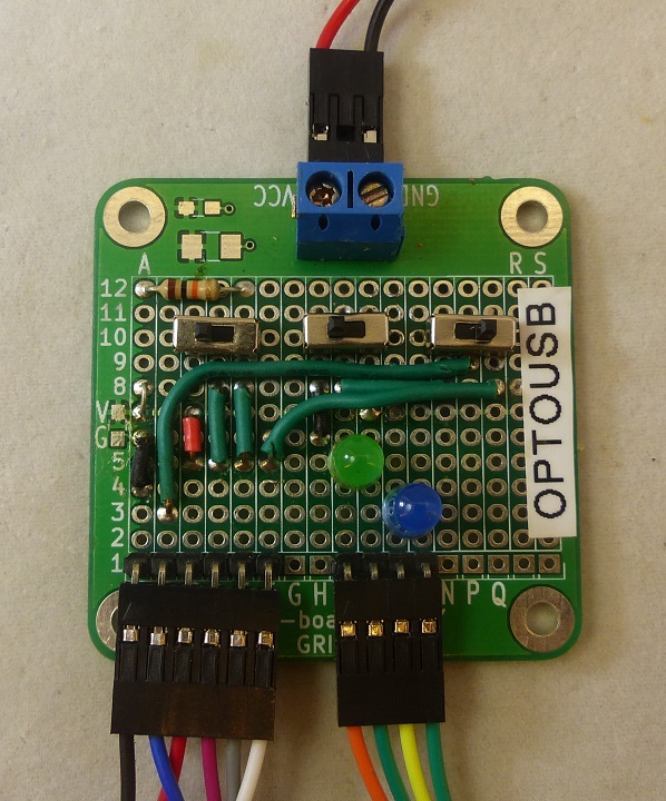
| + | == Factory Acceptance Test == | ||
| + | |||
| + | [[file:OPTOUSB_P18131_720PXV.jpg]] | ||
| + | |||
| + | * Uses dedicated test fixture | ||
| + | ** Built on [[GRID49]] card | ||
| + | ** Card marked OPTOUSB | ||
| + | * Test fixture features | ||
| + | ** 3.3V or 5V power to OptoUSB FTDI TTL level interface | ||
| + | ** Tx/Rx LEDs | ||
| + | ** Loopback select jumpers | ||
| + | |||
| + | === Loopback Select Switches === | ||
| + | |||
| + | [[file:OPTOUSB_P18131_Ann_720PXV.jpg]] | ||
| + | |||
| + | * TX/RX loopback Switch | ||
| + | ** L = Open (Rx pulled up to Vcc) | ||
| + | ** R = Connect TX (out) > RX (in) | ||
| + | * Handshake level Switch | ||
| + | ** L = Active handshake | ||
| + | ** R = Off (Vcc) | ||
| + | * Handshake Switch | ||
| + | ** L = Use Center handshake Switch value | ||
| + | ** R = Loopback CTS > RTS | ||
| + | |||
| + | === Hardware Setup === | ||
| + | |||
| + | * Test "Fixture" | ||
| + | |||
| + | [[file:OPTOUSB_P18128_720PX.jpg]] | ||
| + | |||
| + | * Unit Under Test (UUT) | ||
| + | * Power Supply | ||
| + | ** 5V or 3.3V Power Supply (card build option) | ||
| + | ** Cabled to 5V Terminal block | ||
| + | * FTDI cable | ||
| + | ** From UUT to fixture FTDI jack | ||
| + | ** Left side has Black wire | ||
| + | * LEDs cable | ||
| + | * USB Mini cable to PC | ||
| + | |||
| + | === Test card === | ||
| + | |||
| + | * Run [https://www.chiark.greenend.org.uk/~sgtatham/putty/ puTTY] on PC | ||
| + | ** Find port with Device Manager | ||
| + | ** Baud rate = 115,200 baud | ||
| + | ** Use Hardware handshake RTS/CTS | ||
| + | * Switch settings - Normal operation | ||
| + | ** Left switch in right position (loopback data) | ||
| + | ** Middle switch in left position (handshake = active/ground) | ||
| + | ** Right switch in right position (loopback handshake) | ||
| + | ** Type on keyboard and verify it returns data | ||
| + | ** Both Green and Blue LEDs should blink | ||
| + | * Switch settings - Test Tx/Rx isolation | ||
| + | ** Move left switch to left position | ||
| + | ** Type data nothing should come back | ||
| + | ** Verify Blue LED only blinks | ||
| + | ** Move left switch to right position | ||
| + | * Switch settings - Test RTS/CTS | ||
| + | ** Move right switch to left position (handshake controlled by middle jumper) | ||
| + | ** Type and characters should return | ||
| + | ** Move middle switch to right position (hardware handshake off) | ||
| + | ** Type and nothing should go through | ||
| + | ** Move middle switch to left position (hardware handshake on) | ||
| + | ** Characters that were buffered should come in at once | ||
| + | |||
| + | == Revision History == | ||
| + | |||
| + | Various incarnations of the card | ||
| + | |||
| + | === Rev 5 === | ||
| + | |||
| + | * Adds test point pads | ||
| + | ** Useful for setting TX/RTS Optocoupler output Base resistor values | ||
| + | ** Tune for equal low/high pulse widths | ||
| + | * Cleaned up ref des silkscreen locations, increased sizes | ||
| + | |||
| + | [[FILE:OPTOUSB_REV5_TESTPTS.PNG]] | ||
| + | |||
| + | === Rev 4 === | ||
| + | |||
| + | * Did not build any | ||
| + | |||
| + | === Rev X3 === | ||
| + | |||
| + | * Fixed silkscreen sizes and relocated | ||
| + | * Adds V/G pads on each side | ||
| + | * Add Rx-, TX+ LEDs J2 marking | ||
| + | * Bigger pads for hand soldering discretes | ||
| + | |||
| + | [[FILE:OPTOUSB_REVX3_CAD.PNG]] | ||
| + | |||
| + | === Rework - Rev X1 PWBs === | ||
| + | |||
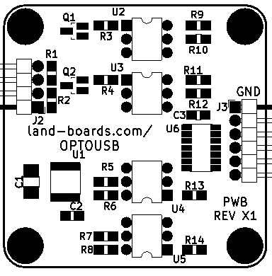
| + | [[file:OPTOUSB_REVX1_CAD.PNG]] | ||
| + | |||
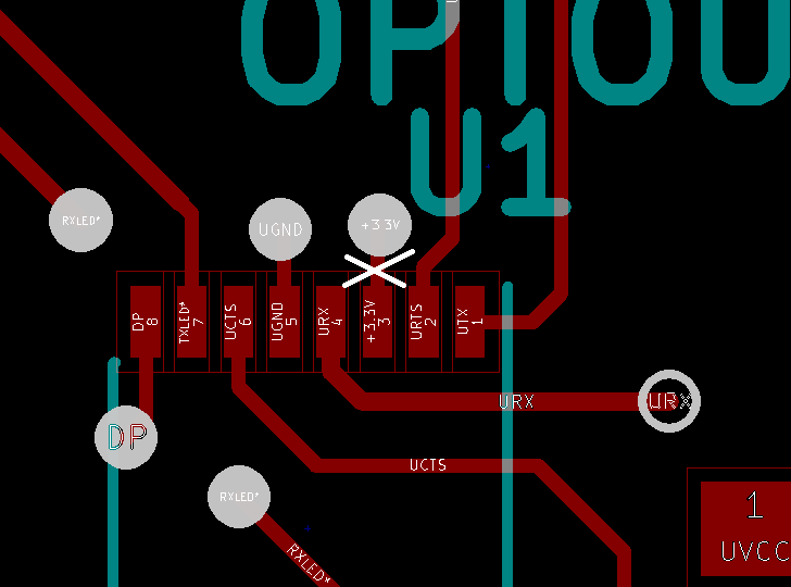
| + | [[file:Rework-U1-3.PNG]] | ||
== Assembly Sheet == | == Assembly Sheet == | ||
* [[OPTOUSB Assembly Sheet]] | * [[OPTOUSB Assembly Sheet]] | ||
Latest revision as of 13:44, 31 October 2022
Contents
- 1 Features
- 2 Block Diagram
- 3 Separate Power Domains
- 4 Connectors
- 5 Drivers
- 6 Layout
- 7 Transfer Rate Characterization
- 8 Opto-Isolator Drive Circuits
- 9 Factory Acceptance Test
- 10 Revision History
- 11 Assembly Sheet
Features
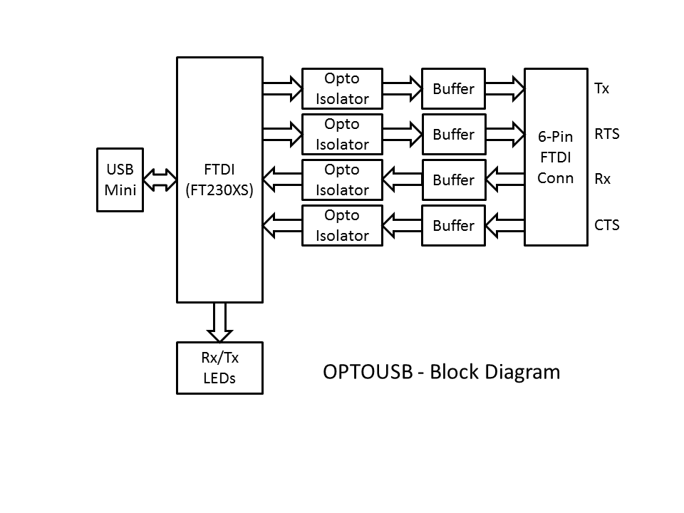
- USB to TTL level Serial (FTDI) Interface
- Genuine FTDI FT230XS part
- Standard FTDI drivers
- Buffered lines on the TTL level side
- Schmidt Trigger
- Voltage level hysteresis
- Improved slew rate
- Schmidt Trigger
- OptoIsolated Connections
- Transmit, Receive, RTS, CTS
- Configured for High Speed Serial
- The Host USB connection is independent of the state of the FTDI side of the interface
- Host side can communicate with the USB host whether or not the target is even powered up
- Target power on/off doesn't cause a USB disconnect - handy for debug
- Fast operation
- 3.3V or 5V FTDI voltage (order option)
- Transmit/Receive LED Connectors
- On-board LED resistors
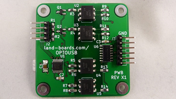
- 49x49mm card
- (4) #4 Mounting Holes
Block Diagram
Separate Power Domains
- The OPTOUSB card has two distinct power domains.
- One of the domains is the USB side where the power comes from the USB connector/cable.
- The other power domain is on the TTL side where the power comes from the FTDI connector.
- This is unlike "normal" FTDI interfaces where the USB connection can power the FTDI side.
- This is the purpose of the optical isolation - to isolate the ground of the USB side from the target (FTDI) side.
Connectors
J1 - Mini USB Connector
- Standard USB Mini connector
J2 - Transmit/Receive LED connections
- PUP0 - LED Pullup to USB Power
- TXLED - Transmit LED
- PUP1 - LED Pullup to USB Power
- RXLED - Receive LED
J3 - FTDI Connector
- Signals are references to external system
- GND
- RTS (In to card)
- VCC (3.3V or 5V) - Power must be supplied to this pin
- Receive (Out from card)
- Transmit (In to card)
- CTS (Out from card)
Drivers
- [ FTDI Drivers]
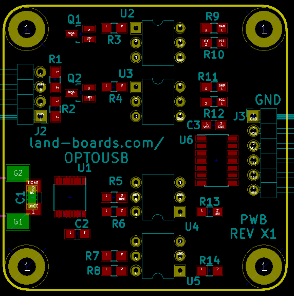
Layout
Transfer Rate Characterization
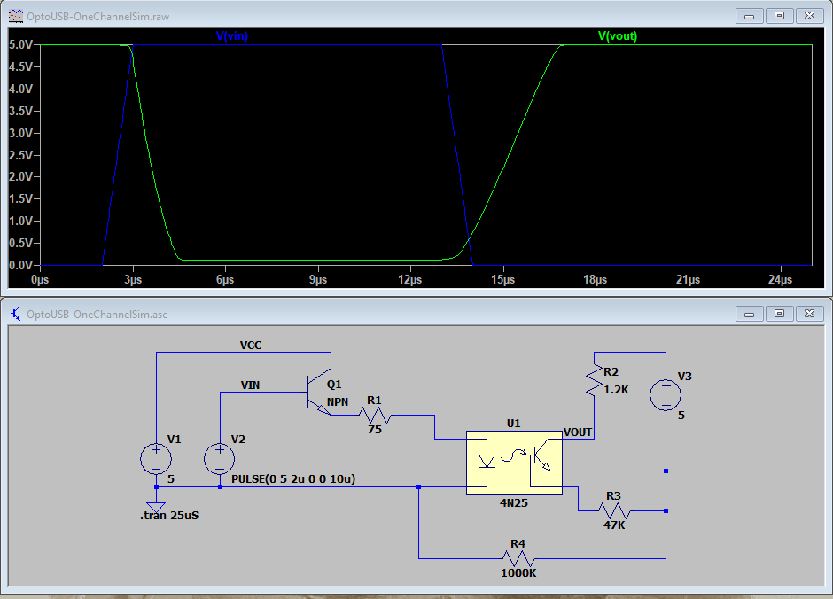
- LTSpice Simulation results
- 8.6uS per bit = 115,200 baud
Opto-Isolator Drive Circuits
- The card has two independent, isolated power domains
- The USB side is powered from the USB 5V
- The FTDI side is powered from external power
- Connected via header or backfeeding the FTDI connector with voltage
- Voltage is one of either 3.3V or 5V
- 4N25 Optoisolator used between the two sides
- Optoisolator has Vf = 1.3V typical
- Optoisolator has 20% CTR (min)
- Optoisolator can be fed with up to 50 mA of drive current
- Set nominal LED drive current at half (25 mA)
USB to FTDI Path
USB Drive Side
- USB side has MMBT3904 (2N3904) transistor for driving the optoisolator
- Vce(Sat) at 10 mA is 0.2V
- Vce(Sat) at 50 mA is 0.3V
- 5V drops are across transistor (0.3V), optoisolator (1.3V) and series resistor
- Opto voltage is 5 - 0.3 - 1.3 = 3.4V
- Opto drive current needs to be 5x the output current (due to the 20% CTR)
- Assume output current (5 mA)
- Optoisolator LED drive current needs to be 25 mA
- 3.4V / .025A = 136 Ohms (Use 150 Ohms for drive series resistor)
- 150 Ohms will be 22.6 mA drive (good compromise drive current value)
- 22.6 mA drive current at 20% CTR will allow collector current to be 4.5 mA
- Transistor base resistor
- HFE(min)=100 @Ice=10mA, HFE(min) = 60 @Ice=50mA
- Use HFE=60
- 4.7V across resistor, HFE=60, Ice =25mA = 11.3K Ohm resistor
- Drive with 5V, 4.7V across 10K is 0.47 mA
- 0.47mA * 60 = 28.2mA (>25 mA)
- HFE(min)=100 @Ice=10mA, HFE(min) = 60 @Ice=50mA
FTDI-Side Collector Pull-up Resistor
- 25 mA into opto
- CTR(min) = 20%
- ~5mA output current
- Optimal resistor value is at cross-over point where the H-L and L-H prop delays trade-off
- ~1.2K
5V FTDI side Collector Pull-up Resistor
- For 5V, that's about 1.2K
- 5V at 1.2K ohms is 4.1 mA
- 4.5 mA collector current (from above)
- 5V at 1.2K ohms is 4.1 mA
- Use 1.2K pull-up from above
3.3V FTDI side Collector Pull-up Resistor
- 4N25 is not characterized for 3.3V operation in the chart but assume the same current
- Vce(sad) = 0.3V
- 3.3-0.3 = 3V
- 3V / 0.0041A = 731 ohms (680 or 750 are standard 5% values that are near)
- Use 820 ohm pull-up
FTDI to USB Path
- Drive FTDI side from 74AC14
- 74AC14 outputs 24 mA Iol or Ioh
5V Drive from FTDI Side
- 150 Ohm series resistor
- 5V-1.3V = 3.7V
- 3.7V / 150 Ohms = 24mA
- Could drop to 180 Ohms for better margin or double up with 2 drivers/series 300 Ohm resistors in future re-design
USB Side Collector Resistor
- Same as above 5V Collector resistor calculation, 1.2K ohms
3.3V Drive from FTDI Side
- 82 Ohm series resistor
- 3.3V-1.3V = 2.0V
- 2.0V / 82 Ohms = 24mA
- Could drop to 100 Ohms for better margin or double up with 2 drivers/series 180 Ohm resistors in future re-design
Optoisolator Speed-ups
- Optoisolators have asymmetric propagation delays Tplh vs Tphl on their outputs
- At Collector Load Value of 1.2K Ohms
- Tplh = 20 uS
- Tphl = 1.5 uS
- This effect limits signal fidelity
- Ideal would be to have matching Tplh and Tphl values
- These can be balanced by adding a resistor from the output side transistor base to ground
- Hard to find "right" value empirically but checking with a scope it's possible to find a good value
- 18 K Ohms for 5V operation
- 15 K Ohms for 3.3V operation
- Top speed is more than 57.6 kbaud with 4N25M optoisolator
- Note: Testing in loopback mode doubles this problem
Optoisolator Improvements
- 4N25M has a low CTR of 20%
- 4N27 is even worse with CTR of 10% - unusable
- CNY17-4X006 has a much better CTR of 160%-320%
- Tested and works reliably up to 200 kbaud with 18K base resistor (above)
- Could also reduce base current
- Might be able to get FTDI side to run at 3.3V or 5V
Factory Acceptance Test
- Uses dedicated test fixture
- Built on GRID49 card
- Card marked OPTOUSB
- Test fixture features
- 3.3V or 5V power to OptoUSB FTDI TTL level interface
- Tx/Rx LEDs
- Loopback select jumpers
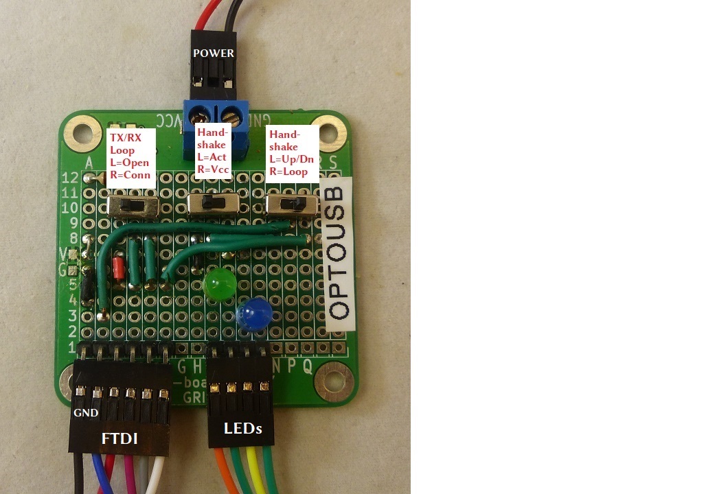
Loopback Select Switches
- TX/RX loopback Switch
- L = Open (Rx pulled up to Vcc)
- R = Connect TX (out) > RX (in)
- Handshake level Switch
- L = Active handshake
- R = Off (Vcc)
- Handshake Switch
- L = Use Center handshake Switch value
- R = Loopback CTS > RTS
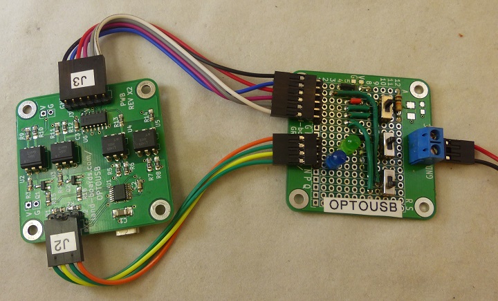
Hardware Setup
- Test "Fixture"
- Unit Under Test (UUT)
- Power Supply
- 5V or 3.3V Power Supply (card build option)
- Cabled to 5V Terminal block
- FTDI cable
- From UUT to fixture FTDI jack
- Left side has Black wire
- LEDs cable
- USB Mini cable to PC
Test card
- Run puTTY on PC
- Find port with Device Manager
- Baud rate = 115,200 baud
- Use Hardware handshake RTS/CTS
- Switch settings - Normal operation
- Left switch in right position (loopback data)
- Middle switch in left position (handshake = active/ground)
- Right switch in right position (loopback handshake)
- Type on keyboard and verify it returns data
- Both Green and Blue LEDs should blink
- Switch settings - Test Tx/Rx isolation
- Move left switch to left position
- Type data nothing should come back
- Verify Blue LED only blinks
- Move left switch to right position
- Switch settings - Test RTS/CTS
- Move right switch to left position (handshake controlled by middle jumper)
- Type and characters should return
- Move middle switch to right position (hardware handshake off)
- Type and nothing should go through
- Move middle switch to left position (hardware handshake on)
- Characters that were buffered should come in at once
Revision History
Various incarnations of the card
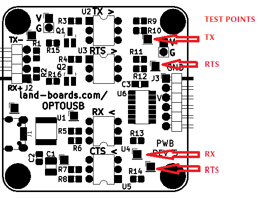
Rev 5
- Adds test point pads
- Useful for setting TX/RTS Optocoupler output Base resistor values
- Tune for equal low/high pulse widths
- Cleaned up ref des silkscreen locations, increased sizes
Rev 4
- Did not build any
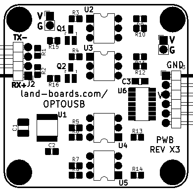
Rev X3
- Fixed silkscreen sizes and relocated
- Adds V/G pads on each side
- Add Rx-, TX+ LEDs J2 marking
- Bigger pads for hand soldering discretes

