RPIO-TINY-2
Raspberry Pi Sensor Connection Card
Card that allows 3.3V and 5V devices to be easily connected to the Raspberry Pi.
Board Design
This board is modeled on the Arduino Sensor Shields, also known as GVS shields. Arduino Sensor Shields bring out the pins of the Arduino to GVS (set of Ground, Voltage and Signal) pins. Unfortunately, the Raspberry Pi can't work with the same 5V GVS sensors and devices as the Arduino since the Raspberry Pi has 3.3V I/O.
The RPIO-TINY-2 card allows the Raspberry Pi to communicate with the same 5V sensors by performing voltage translation from the 3.3V of the Raspberry Pi to 5V.
Features
- All Raspberry Pi I/O lines
- 8-bit bidirectional 3.3V to 5V level translator
- Fuses on 3.3V and 5V power lines
Raspberry Pi I/O lines
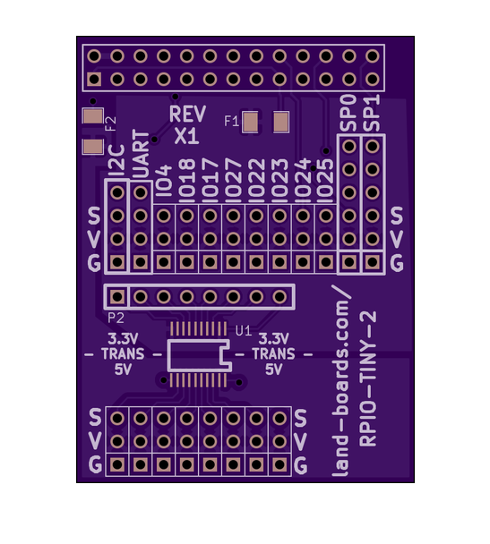
All of the Raspberry Pi I/O connections are brought to GVS connectors. This is:
- (8) GPIO lines on GVS connectors
- (2) SPI interfaces (can be configured as 5 GPIO lines)
- (1) UART interface (can be configured as 2 GPIO lines)
- (1) I2C interface(can be configured as 2 GPIO lines)
Level translators
The board uses an 8-bit wide Texas Instrument TXS0108 voltage translator to convert up to 8 of the 3.3V I/O lines to 5V I/O levels.
Voltage Translators Features
- No Direction-Control Signal Needed
- Max Data Rates
- 60 Mbps (Push Pull)
- 2 Mbps (Open Drain)
- 1.2 V to 3.6 V on A Port and 1.65 V to 5.5 V on
- B Port (VCCA ≤ VCCB)
- No Power-Supply Sequencing Required –
- Either VCCA or VCCB Can Be Ramped First
- Latch-Up Performance Exceeds 100 mA Per JESD 78, Class II
- ESD Protection Exceeds JESD 22 (A Port)
- 2000-V Human-Body Model (A114-B)
- 150-V Machine Model (A115-A)
- 1000-V Charged-Device Model (C101)
- IEC 61000-4-2 ESD (B Port)
- ±6-kV Air-Gap Discharge
- ±8-kV Contact Discharge
Voltage Translators Architecture
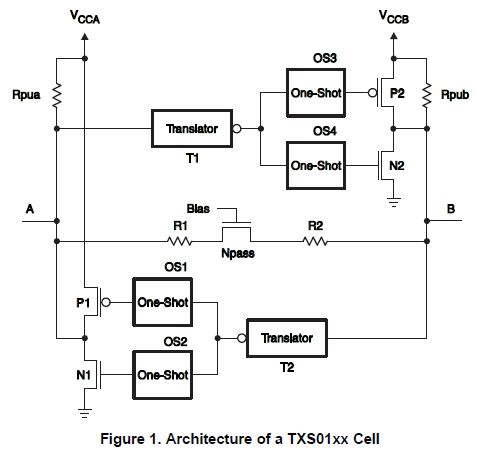
The TXS0108E can be used in level-translation applications for interfacing devices or systems operating at different interface voltages with one another. The TXS0108E is ideal for use in applications where an open-drain driver is connected to the data I/Os. The TXS0108E can also be used in applications where a push-pull driver is connected to the data I/Os, but the TXB0104 might be a better option for such push-pull applications. The TXS0108E device is a semi-buffered auto-direction-sensing voltage translator design is optimized for translation applications (e.g. MMC Card Interfaces) that require the system to start out in a low-speed open-drain mode and then switch to a higher speed push-pull mode.
To address these application requirements, a semi-buffered architecture design is used and is illustrated above (see Figure 1). Edge-rate accelerator circuitry (for both the high-to-low and low-to-high edges), a High-Ron n-channel pass-gate transistor (on the order of 300 Ω to 500 Ω) and pull-up resistors (to provide DC-bias and drive capabilities) are included to realize this solution. A direction-control signal (to control the direction of data flow from A to B or from B to A) is not needed. The resulting implementation supports both low-speed open-drain operation as well as high-speed push-pull operation.
When transmitting data from A to B ports, during a rising edge the One-Shot (OS3) turns on the PMOS transistor (P2) for a short-duration and this speeds up the low-to-high transition. Similarly, during a falling edge, when transmitting data from A to B, the One-Shot (OS4) turns on NMOS transistor (N2) for a short-duration and this speeds up the high-to-low transition. The B-port edge-rate accelerator consists of one-shots OS3 and OS4, Transistors P2 and N2 and serves to rapidly force the B port high or low when a corresponding transition is detected on the A port.
When transmitting data from B to A ports, during a rising edge the One-Shot (OS1) turns on the PMOS transistor (P1) for a short-duration and this speeds up the low-to-high transition. Similarly, during a falling edge, when transmitting data from B to A, the One-Shot (OS2) turns on NMOS transistor (N1) for a short-duration and this speeds up the high-to-low transition. The A-port edge-rate accelerator consists of one-shots OS1 and OS2, Transistors P1 and N1 components and form the edge-rate accelerator and serves to rapidly force the A port high or low when a corresponding transition is detected on the B port.
Fuses
- The board has Resettable fuses on the 3.3V and 5V from the Raspberry Pi.
- These fuses protect your Raspberry Pi from overloads.
- These fuses are 1/2 Amp PTC fuses.
- PTC fuses have certain advantages (they are self healing) and disadvantages (they are not like a wire fuse which acts like a switch).
- If you trust your wiring you may choose to solder a wire over the fuse.
- Care should be taken when doing so.
Connectors
Raspberry Pi GPIO Connector
File:Raspberry-pi-rev2-gpio-pinout.jpg
3.3V Connectors
The following are all 3.3VDC connections.
I2C bus
- GND
- 3.3V
- SDA
- SCL
UART I/F
- GND
- 3.3V
- TxD
- RxD
IO_4 GVS
- GND
- 3.3V
- GPIO_4
IO_18 GVS
- GND
- 3.3V
- GPIO_18
IO_17 GVS
- GND
- 3.3V
- GPIO_17
IO_27 GVS
GND 3.3V GPIO_27 IO_23 GVS GND 3.3V GPIO_23 IO_22 GVS GND 3.3V GPIO_22 IO_24 GVS GND 3.3V GPIO_24 IO_25 GVS GND 3.3V GPIO_25 SPI0 (Serial Peripheral Interface) GND 3.3V MOSI MISO SCK CE0 SPI1 (Serial Peripheral Interface) GND 3.3V MOSI MISO SCK CE1 P2 - Voltage translator, 3.3V side This connector has the 8-bits of the 3.3V side of the voltage translator. Use female to female cables to connect these pins to the 3.3V GPIO lines.
P2-1 = Bit 1 P2-2 = Bit 2 P2-3 = Bit 3 P2-4 = Bit 4 P2-5 = Bit 5 P2-6 = Bit 6 P2-7 = Bit 7 P2-8 = Bit 8 5V Connectors The following are 5V connectors.
V5-1 - GVS connector, 5V side Ground +5V Bit1 V5-2 - GVS connector, 5V side Ground +5V Bit2 V5-3 - GVS connector, 5V side Ground +5V Bit3 V5-4 - GVS connector, 5V side Ground +5V Bit4 V5-5 - GVS connector, 5V side Ground +5V Bit5 V5-6 - GVS connector, 5V side Ground +5V Bit6 V5-7 - GVS connector, 5V side Ground +5V Bit7 V5-8 - GVS connector, 5V side Ground +5V Bit8 Layout RPIO-TINY-2-CAD-X1.PNG
Assembly Sheet RPIO-TINY-2 Configuration Sheet Design Validation Testing Based on RASPI-PLUS-GVS-CFG DVT
Factory Acceptance Tests (FAT) Hardware FAT requires the following:
Raspberry Pi (RasPi) Power supply for Raspberry Pi (5V at 1 Amp min) with Micro USB connector Monitor, Keyboard or Ethernet cable and laptop running puTTY Test Software loaded onto RasPi (1) LED-Test-2 card 1 LED Jumpers (female-to-female) Daisy-chain cables 8-pin female-female jumper cables Unit Under Test (UUT) Preliminary Install UUT onto RasPi Install Cables Power up card Log into RasPi GVS Connector - Daisy-chain and Translator Tests cd ~/RasPi/RPIO-TINY-2 sudo python fastTest-RPT2.py
GVS Connector - LED Blink Tests cd ~/RasPi/RPIO-TINY-2 sudo python blinkLEDs-RPIO-TINY-2.py

