Difference between revisions of "Multicomp in a Box"
Jump to navigation
Jump to search
Blwikiadmin (talk | contribs) |
Blwikiadmin (talk | contribs) |
||
| Line 1: | Line 1: | ||
== Features == | == Features == | ||
| − | * This is an FPGA card in a box | + | * This is an FPGA card in a box with support hardware |
** Provides a standardized interface for all FPGA Retrocomputer builds | ** Provides a standardized interface for all FPGA Retrocomputer builds | ||
Revision as of 19:59, 18 February 2022
Contents
Features
- This is an FPGA card in a box with support hardware
- Provides a standardized interface for all FPGA Retrocomputer builds
Retro-Computer Builds
Multicomp Builds
- 6502
- OSI BASIC
- UK101 / Ohio Scientific (OSI) C1P
- 6809
- BASIC
- Neal Crook Multiple OS
- Z80
- CP/M (various builds)
Other Builds
- 6800
- MIKBUG
- 68000
- Teeside 2 (TS2) compatible
- TS2BUG ROM
- TUTOR ROM
- Teeside 2 (TS2) compatible
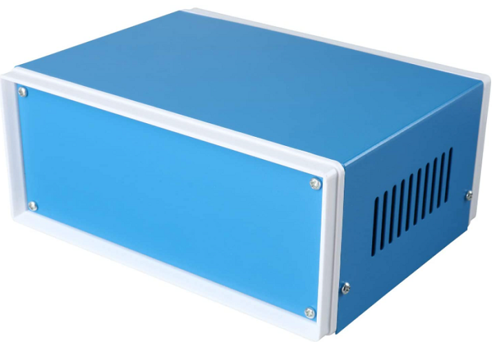
Enclosure
Card Set
- RETRO-EP4CE15 FPGA Baseboard
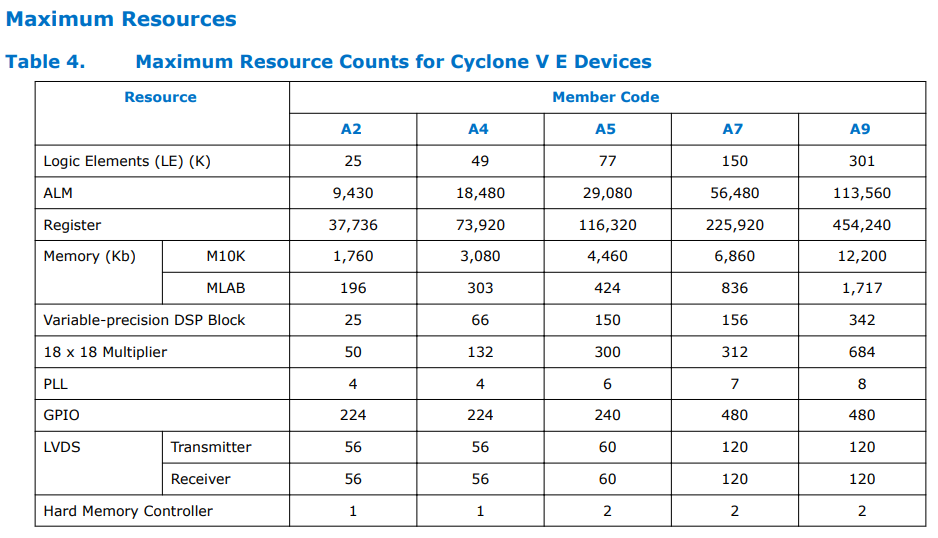
- QM Tech Cyclone V FPGA Board
- SD CARD X49
- Slide switches card - Using 4 slide switches
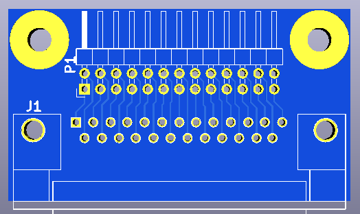
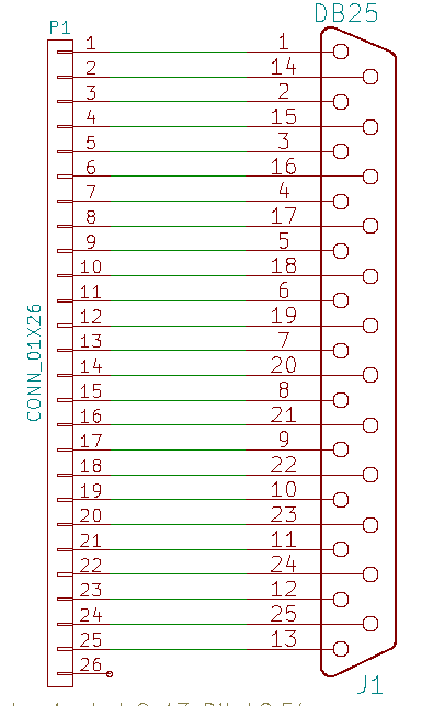
- DB25-02 - DB-25
- Power Distribution card
- Reset switch
- Mounted to front panel
- On FPGA Pin_N16 (J3-6)
- USB Blaster - Remove from case - Opening in enclosure to access USB connector
QM Tech Cyclone V FPGA Board Features
- QM Tech Cyclone V FPGA Board
- QMTECH Altera Intel FPGA Core Board Cyclone V CycloneV 5CEFA2F23 SDRAM
- QMTECH GitHub page
- On-Board FPGA: 5CEFA2F23I7N
- On-Board FPGA external crystal frequency: 50MHz
- 5CEFA2F23 has rich RAM resource up to 1,760Kb
- 5CEFA2F23 has 25K logic cells
- On-Board Micron MT25QL128A SPI Flash, 16M bytes for user configuration code
- On-Board Winbond 32MB SDRAM, W9825G6KH-6
- On-Board 3.3V power supply for FPGA by using MP2315 wide input range DC/DC
- 5CEFA2F23 core board has two 64p, 2.54mm pitch headers for extending 108 user IOs. All 108 user IOs are precisely designed with length matching
- 5CEFA2F23 core board has 3 user switches
- 5CEFA2F23 core board has 2 user LEDs
- 5CEFA2F23 core board has JTAG interface, by using 10p, 2.54mm pitch header
- 5CEFA2F23 core board PCB size is: 6.7cm x 8.4cm
- Default power source for board is: 1A@5V DC, the DC header type: DC-050, 5.5mmx2.1mm
Cyclone V_FPGA Resources
- 176 1Kx10 RAM blocks
- Power LED - D4 (On when 5V is applied)
- User LED - LED_D5 - FPGA Pin_D17 (pull low to illuminate LED)
- KEY0 - SW1 - FPGA Pin_AB13
- RESET_N- SW2 - FPGA PIN_V18
- nCONFIG - SW3 - FPGA PIN_A4
- JP5 - 5V
- Clock - FPGA PIN_M9
Pin List (5CEFA2F23I7)
set_global_assignment -name FAMILY "Cyclone V"
set_global_assignment -name DEVICE 5CEFA2F23I7
set_global_assignment -name TOP_LEVEL_ENTITY Microcomputer
set_global_assignment -name ORIGINAL_QUARTUS_VERSION "13.0 SP1"
set_global_assignment -name PROJECT_CREATION_TIME_DATE "17:55:48  OCTOBER 20, 2013"
set_global_assignment -name LAST_QUARTUS_VERSION "21.1.0 Lite Edition"
set_global_assignment -name PROJECT_OUTPUT_DIRECTORY output_files
set_global_assignment -name MIN_CORE_JUNCTION_TEMP "-40"
set_global_assignment -name MAX_CORE_JUNCTION_TEMP 100
set_global_assignment -name ERROR_CHECK_FREQUENCY_DIVISOR 1
set_global_assignment -name PARTITION_NETLIST_TYPE SOURCE -section_id Top
set_global_assignment -name PARTITION_FITTER_PRESERVATION_LEVEL PLACEMENT_AND_ROUTING -section_id Top
set_global_assignment -name PARTITION_COLOR 16764057 -section_id Top
set_global_assignment -name STRATIX_DEVICE_IO_STANDARD "3.3-V LVTTL"
set_global_assignment -name OPTIMIZE_HOLD_TIMING "IO PATHS AND MINIMUM TPD PATHS"
set_global_assignment -name OPTIMIZE_MULTI_CORNER_TIMING ON
set_global_assignment -name POWER_PRESET_COOLING_SOLUTION "23 MM HEAT SINK WITH 200 LFPM AIRFLOW"
set_global_assignment -name POWER_BOARD_THERMAL_MODEL "NONE (CONSERVATIVE)"
set_global_assignment -name USE_CONFIGURATION_DEVICE ON
set_global_assignment -name RESERVE_ALL_UNUSED_PINS "AS INPUT TRI-STATED WITH WEAK PULL-UP"
set_global_assignment -name VHDL_INPUT_VERSION VHDL_1993
set_global_assignment -name VHDL_SHOW_LMF_MAPPING_MESSAGES OFF
set_global_assignment -name DEVICE_FILTER_SPEED_GRADE 7
set_global_assignment -name TIMING_ANALYZER_MULTICORNER_ANALYSIS ON
set_global_assignment -name SMART_RECOMPILE ON
set_global_assignment -name NUM_PARALLEL_PROCESSORS 4
# Clock (int 50 MHz osc) and reset (on front panel)
set_location_assignment PIN_M9 -to clk
set_location_assignment PIN_N16 -to n_reset
set_instance_assignment -name WEAK_PULL_UP_RESISTOR ON -to n_reset
# USB-Serial
set_location_assignment PIN_B11 -to cts1
set_location_assignment PIN_F10 -to rts1
set_location_assignment PIN_C11 -to rxd1
set_location_assignment PIN_G10 -to txd1
set_instance_assignment -name WEAK_PULL_UP_RESISTOR ON -to rxd1
# SRAM
set_location_assignment PIN_E2 -to n_sRamCS
set_location_assignment PIN_L2 -to n_sRamOE
set_location_assignment PIN_D6 -to n_sRamWE
set_location_assignment PIN_E9 -to sramAddress[19]
set_location_assignment PIN_B5 -to sramAddress[18]
set_location_assignment PIN_B6 -to sramAddress[17]
set_location_assignment PIN_A7 -to sramAddress[16]
set_location_assignment PIN_A10 -to sramAddress[15]
set_location_assignment PIN_A8 -to sramAddress[14]
set_location_assignment PIN_B7 -to sramAddress[13]
set_location_assignment PIN_A5 -to sramAddress[12]
set_location_assignment PIN_D9 -to sramAddress[11]
set_location_assignment PIN_C6 -to sramAddress[10]
set_location_assignment PIN_E7 -to sramAddress[9]
set_location_assignment PIN_G2 -to sramAddress[8]
set_location_assignment PIN_N2 -to sramAddress[7]
set_location_assignment PIN_U2 -to sramAddress[6]
set_location_assignment PIN_W2 -to sramAddress[5]
set_location_assignment PIN_Y3 -to sramAddress[4]
set_location_assignment PIN_U1 -to sramAddress[3]
set_location_assignment PIN_N1 -to sramAddress[2]
set_location_assignment PIN_L1 -to sramAddress[1]
set_location_assignment PIN_G1 -to sramAddress[0]
set_location_assignment PIN_C1 -to sramData[0]
set_location_assignment PIN_G6 -to sramData[1]
set_location_assignment PIN_G8 -to sramData[2]
set_location_assignment PIN_F7 -to sramData[3]
set_location_assignment PIN_H8 -to sramData[4]
set_location_assignment PIN_H6 -to sramData[5]
set_location_assignment PIN_C2 -to sramData[6]
set_location_assignment PIN_D3 -to sramData[7]
# External SD Card
set_location_assignment PIN_M22 -to sdCardCS
set_location_assignment PIN_L18 -to sdCardMISO
set_location_assignment PIN_L22 -to sdCardMOSI
set_location_assignment PIN_L19 -to sdCardSCLK
set_instance_assignment -name WEAK_PULL_UP_RESISTOR ON -to sdCardMISO
# set_location_assignment PIN_B12 -to sdCardDet_n
# set_location_assignment PIN_D17 -to driveLED
# Video
set_location_assignment PIN_A15 -to hSync
set_location_assignment PIN_D12 -to videoR1
set_location_assignment PIN_E12 -to videoR0
set_location_assignment PIN_C13 -to videoG1
set_location_assignment PIN_D13 -to videoG0
set_location_assignment PIN_A13 -to videoB1
set_location_assignment PIN_B13 -to videoB0
set_location_assignment PIN_A14 -to vSync
# PS/2
set_location_assignment PIN_AA2 -to ps2Clk
set_location_assignment PIN_AA1 -to ps2Data
set_instance_assignment -name WEAK_PULL_UP_RESISTOR ON -to ps2Clk
set_instance_assignment -name WEAK_PULL_UP_RESISTOR ON -to ps2Data
# SDRAM
set_location_assignment PIN_AB11 -to sdRamClk
set_location_assignment PIN_V9 -to sdRamClkEn
set_location_assignment PIN_AA7 -to n_sdRamCas
set_location_assignment PIN_AB5 -to n_sdRamCe
set_location_assignment PIN_AB6 -to n_sdRamRas
set_location_assignment PIN_W9 -to n_sdRamWe
set_location_assignment PIN_AB7 -to o_sdram_ldqm
set_location_assignment PIN_V10 -to o_sdram_udqm
set_location_assignment PIN_P9 -to sdRamAddr[14]
set_location_assignment PIN_T7 -to sdRamAddr[13]
set_location_assignment PIN_Y9 -to sdRamAddr[12]
set_location_assignment PIN_T9 -to sdRamAddr[11]
set_location_assignment PIN_R6 -to sdRamAddr[10]
set_location_assignment PIN_W8 -to sdRamAddr[9]
set_location_assignment PIN_T8 -to sdRamAddr[8]
set_location_assignment PIN_U8 -to sdRamAddr[7]
set_location_assignment PIN_V6 -to sdRamAddr[6]
set_location_assignment PIN_U7 -to sdRamAddr[5]
set_location_assignment PIN_U6 -to sdRamAddr[4]
set_location_assignment PIN_N6 -to sdRamAddr[3]
set_location_assignment PIN_N8 -to sdRamAddr[2]
set_location_assignment PIN_P7 -to sdRamAddr[1]
set_location_assignment PIN_P8 -to sdRamAddr[0]
set_location_assignment PIN_P12 -to sdRamData[15]
set_location_assignment PIN_R12 -to sdRamData[14]
set_location_assignment PIN_U12 -to sdRamData[13]
set_location_assignment PIN_R11 -to sdRamData[12]
set_location_assignment PIN_R10 -to sdRamData[11]
set_location_assignment PIN_U11 -to sdRamData[10]
set_location_assignment PIN_T10 -to sdRamData[9]
set_location_assignment PIN_U10 -to sdRamData[8]
set_location_assignment PIN_AA8 -to sdRamData[7]
set_location_assignment PIN_AB8 -to sdRamData[6]
set_location_assignment PIN_AA9 -to sdRamData[5]
set_location_assignment PIN_Y10 -to sdRamData[4]
set_location_assignment PIN_AB10 -to sdRamData[3]
set_location_assignment PIN_AA10 -to sdRamData[2]
set_location_assignment PIN_Y11 -to sdRamData[1]
set_location_assignment PIN_AA12 -to sdRamData[0]
# I/O Pins
set_location_assignment PIN_AB15 -to IO_PIN[3]
set_location_assignment PIN_AA15 -to IO_PIN[4]
set_location_assignment PIN_Y14 -to IO_PIN[5]
set_location_assignment PIN_Y15 -to IO_PIN[6]
set_location_assignment PIN_AB17 -to IO_PIN[7]
set_location_assignment PIN_AB18 -to IO_PIN[8]
set_location_assignment PIN_Y16 -to IO_PIN[9]
set_location_assignment PIN_Y17 -to IO_PIN[10]
set_location_assignment PIN_AA17 -to IO_PIN[11]
set_location_assignment PIN_AA18 -to IO_PIN[12]
set_location_assignment PIN_AA19 -to IO_PIN[13]
set_location_assignment PIN_AA20 -to IO_PIN[14]
set_location_assignment PIN_Y19 -to IO_PIN[15]
set_location_assignment PIN_Y20 -to IO_PIN[16]
set_location_assignment PIN_AB20 -to IO_PIN[17]
set_location_assignment PIN_AB21 -to IO_PIN[18]
set_location_assignment PIN_AB22 -to IO_PIN[19]
set_location_assignment PIN_AA22 -to IO_PIN[20]
set_location_assignment PIN_Y22 -to IO_PIN[21]
set_location_assignment PIN_W22 -to IO_PIN[22]
set_location_assignment PIN_W21 -to IO_PIN[23]
set_location_assignment PIN_Y21 -to IO_PIN[24]
set_location_assignment PIN_V21 -to IO_PIN[25]
set_location_assignment PIN_U22 -to IO_PIN[26]
set_location_assignment PIN_W19 -to IO_PIN[27]
set_location_assignment PIN_V20 -to IO_PIN[28]
set_location_assignment PIN_U20 -to IO_PIN[29]
set_location_assignment PIN_U21 -to IO_PIN[30]
set_location_assignment PIN_T22 -to IO_PIN[31]
set_location_assignment PIN_R22 -to IO_PIN[32]
set_location_assignment PIN_R21 -to IO_PIN[33]
set_location_assignment PIN_P22 -to IO_PIN[34]
set_location_assignment PIN_T19 -to IO_PIN[35]
set_location_assignment PIN_T20 -to IO_PIN[36]
set_location_assignment PIN_P17 -to IO_PIN[37]
set_location_assignment PIN_P16 -to IO_PIN[38]
set_location_assignment PIN_N21 -to IO_PIN[39]
set_location_assignment PIN_N20 -to IO_PIN[40]
set_location_assignment PIN_M20 -to IO_PIN[41]
set_location_assignment PIN_M21 -to IO_PIN[42]
set_location_assignment PIN_N19 -to IO_PIN[43]
set_location_assignment PIN_M18 -to IO_PIN[44]
#
set_global_assignment -name VHDL_FILE Microcomputer.vhd
set_global_assignment -name VHDL_FILE "../../../MultiComp (VHDL Template)/Components/CPU/Z80/T80s.vhd"
set_global_assignment -name VHDL_FILE "../../../MultiComp (VHDL Template)/Components/CPU/Z80/T80_Reg.vhd"
set_global_assignment -name VHDL_FILE "../../../MultiComp (VHDL Template)/Components/CPU/Z80/T80_Pack.vhd"
set_global_assignment -name VHDL_FILE "../../../MultiComp (VHDL Template)/Components/CPU/Z80/T80_MCode.vhd"
set_global_assignment -name VHDL_FILE "../../../MultiComp (VHDL Template)/Components/CPU/Z80/T80_ALU.vhd"
set_global_assignment -name VHDL_FILE "../../../MultiComp (VHDL Template)/Components/CPU/Z80/T80.vhd"
set_global_assignment -name VHDL_FILE "../../../MultiComp (VHDL Template)/Components/ROMs/Z80/Z80_CMON/Z80_CMON_ROM.vhd"
set_global_assignment -name SOURCE_FILE "../../../MultiComp (VHDL Template)/Components/ROMs/Z80/Z80_CMON/Z80_CMON_ROM.cmp"
set_global_assignment -name VHDL_FILE "../../../MultiComp (VHDL Template)/Components/TERMINAL/DisplayRam2K.vhd"
set_global_assignment -name VHDL_FILE "../../../MultiComp (VHDL Template)/Components/TERMINAL/DisplayRam1K.vhd"
set_global_assignment -name VHDL_FILE "../../../MultiComp (VHDL Template)/Components/TERMINAL/CGABoldRomReduced.vhd"
set_global_assignment -name VHDL_FILE "../../../MultiComp (VHDL Template)/Components/TERMINAL/CGABoldRom.vhd"
set_global_assignment -name VHDL_FILE "../../../MultiComp (VHDL Template)/Components/UART/Previous_Revisions/bufferedUART_MJC.vhd"
set_global_assignment -name VHDL_FILE ../Components/BRG/brg.vhd
set_global_assignment -name VHDL_FILE "../../../MultiComp (VHDL Template)/Components/SDCARD/sd_controller_High_Speed.vhd"
set_global_assignment -name VHDL_FILE ../Components/TERMINAL/SBCTextDisplayRGB.vhd
set_global_assignment -name VHDL_FILE ../Components/TERMINAL/keyMapRom.vhd
set_global_assignment -name VHDL_FILE "../../../MultiComp (VHDL Template)/Components/Memory_Mappers/MMU4/MMU4.vhd"
#
set_global_assignment -name SOURCE_FILE Microcomputer.qsf
set_global_assignment -name SOURCE_FILE db/Microcomputer.cmp.rdb
set_global_assignment -name CDF_FILE ../../../../gameserver/QuartusII/Microcomputer_VGA/output_files/Chain1.cdf
set_instance_assignment -name PARTITION_HIERARCHY root_partition -to | -section_id Top
Power
- 5V Power comes from the USB
- 3.3V regulator on the RETRO-EP4CE15 Card
- H2 pins 2-3 shorted on the RETRO-EP4CE15 card
- Set to route 3.3V to the I/O connector
Cabling
SD Card
- SD Card
- Install J3 on SD Card
- Runs card off 3.3V
| J1 PIN | SIGNAL | COLOR | SD PIN | FPGA Pin | DIR |
|---|---|---|---|---|---|
| 2 | 3.3V | ORG | 7 | VREG 3.3V | OUT (PWR) |
| 45 | sdSCLK | GRY | 3 | L19 | OUT |
| 46 | sdMISO | BLU | 2 | L18 | IN |
| 47 | sdMOSI | WHT | 4 | L22 | OUT |
| 48 | sdCS | VIO | 5 | M22 | OUT |
| 49 | GND | GRN | 1 | GND | OUT (PWR) |


