Difference between revisions of "OptoOut8-I2C"
Jump to navigation
Jump to search
Blwikiadmin (talk | contribs) |
Blwikiadmin (talk | contribs) |
||
| Line 425: | Line 425: | ||
=== Setup Power and Ground === | === Setup Power and Ground === | ||
| − | * | + | * Drive Grounds to Digio32 channels 0-7 (dec) |
** I from top menu accesses the DIGIO32-I2C | ** I from top menu accesses the DIGIO32-I2C | ||
*** L command sets pins to low | *** L command sets pins to low | ||
| Line 444: | Line 444: | ||
</pre> | </pre> | ||
| − | * | + | * Drive Powers to Digio32 channels 8-15 (dec) |
** I from top menu accesses the DIGIO32-I2C | ** I from top menu accesses the DIGIO32-I2C | ||
*** H command sets pins to low | *** H command sets pins to low | ||
Revision as of 13:00, 13 March 2022
Contents
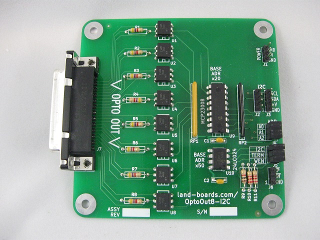
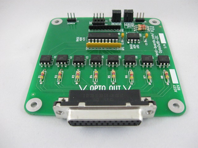
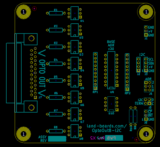
Eight Channel Optically Isolated Output Card with I2C bus
Features
- Eight optically-isolated output channels on card
- (8) 4N25 optoisolators
- MCP23008 I2C Parallel I/O
- I2C (Two Wire interface)
- 100/400 KHZ operation
- 25mA sink/source capability per I/O
- Jumper selectable 2.2K Ohm terminators
- 3-bit address (Jumper selectable) - Up to 8 boards
- Single 4-pin host interface connector (Ground, Power, Clock, Data)
- 24LC024 Personality EEPROM
- Write protect jumper
- 5V operation
- Compatible with Arduino, Raspberry Pi, BeagleBone Black
- DB-25F connector for rugged applications
- 95x95mm form factor
- (4) 6-32 mounting holes - one on each corner
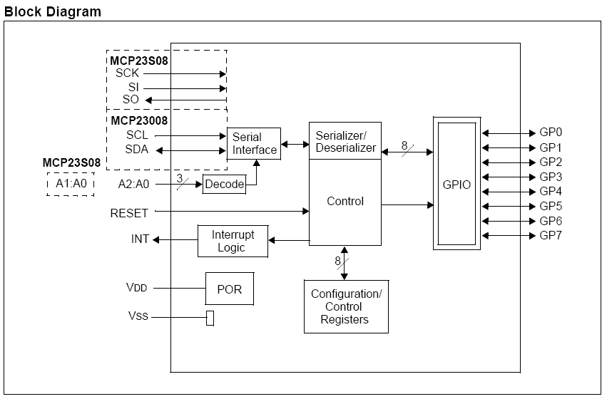
MCP23008 Block Diagram
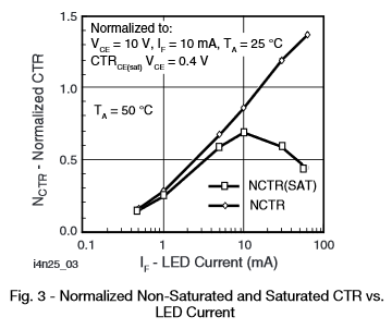
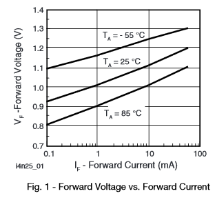
Optocoupler Performance
- 4N25 Optocoupler
- DC Current Transfer Ratio
- Current Transfer ratio curve
- LED Current vs voltage
- Output transistor capacitance
- Switching Time
Opto Characteristics
Current Transfer Ratio	10.00%	min
Vcc	5	V	3.3	V
Vf(Diode)	1.25	V	1.25	V
Res series LED	330	Ohms	330	Ohms
If (LED)	0.0113636364	A	0.0062121212	A
CTR	0.6	A/A	0.2	A/A
Current Trans CE	0.0068181818	A	0.0012424242	A
Res (load pullup)	4700	Ohms	4700	Ohms
Vce	0.2	V	0.2	V
V load side	5	V	5	V
Iload	0.0010212766		0.0010212766
Connectors
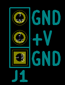
J1 - Power
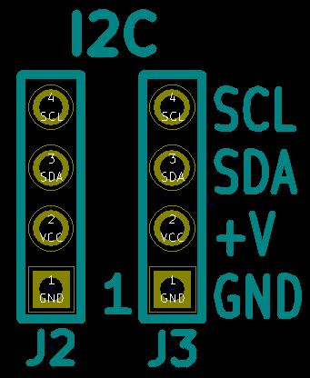
J2-J3 - I2C
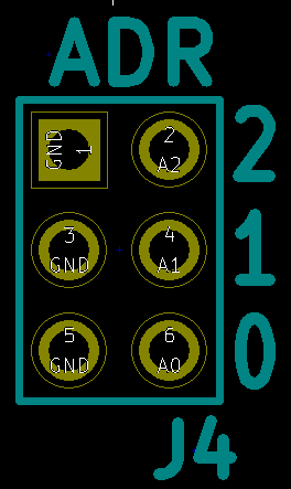
J4 - I2C Address Select Jumpers
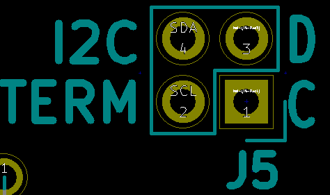
J5 - I2C Termination Jumpers
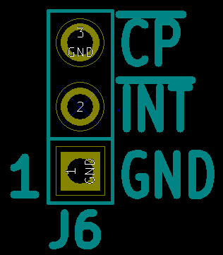
J6 - Card Present/Interrupt
- GND
- INT
- CP - Card present (pulled low)
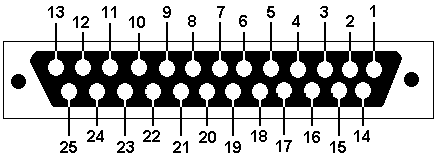
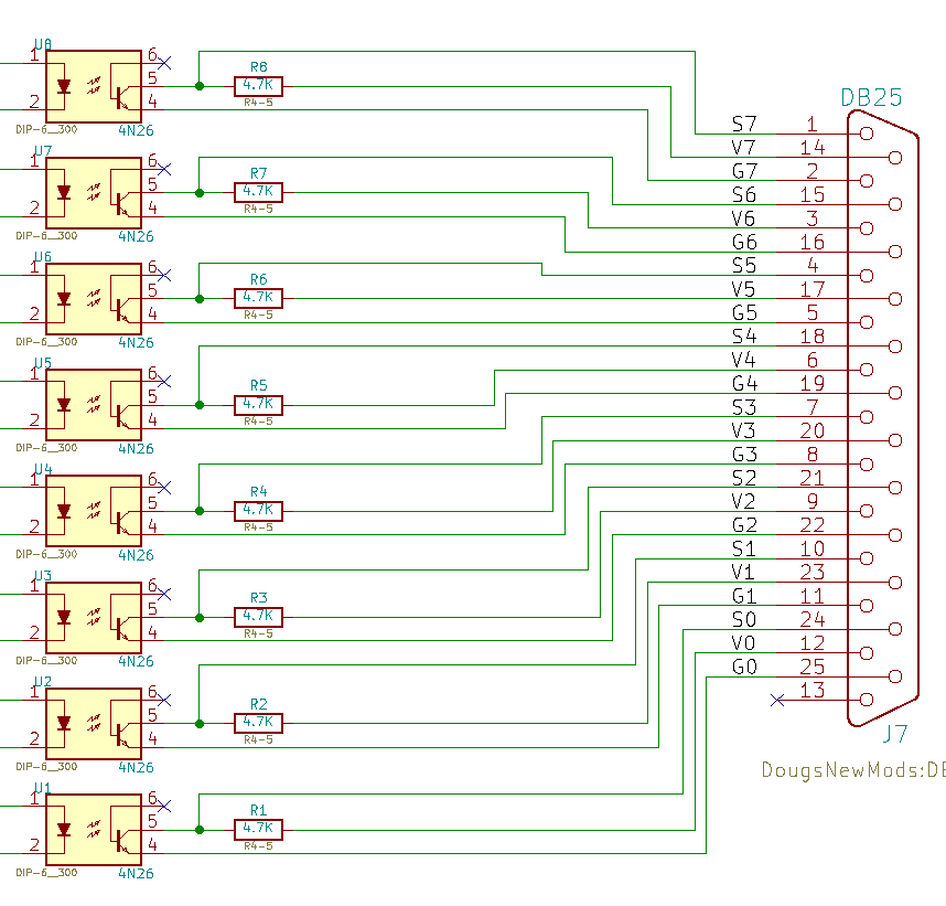
J7 - I/O connector
DB-25 Female
| OptoOut | OptoOut | DB25RIB | DIGIO32 | DB37RIB | OptoOut | OptoOut | DB25RIB | DIGIO32 | DB37RIB | |
|---|---|---|---|---|---|---|---|---|---|---|
| Pin | Descr | Pin_26 | Descr | Pin_40 | Pin | Descr | Pin_26 | Descr | Pin_40 | |
| 1 | S7 | 1 | C1PA7 | 18 | 14 | V7 | 2 | C0PB7 | 20 | |
| 2 | G7 | 3 | C0PA7 | 35 | 15 | S6 | 4 | C1PA6 | 16 | |
| 3 | V6 | 5 | C0PB6 | 22 | 16 | G6 | 6 | C0PA6 | 33 | |
| 4 | S5 | 7 | C1PA5 | 14 | 17 | V5 | 8 | C0PB5 | 24 | |
| 5 | G5 | 9 | C0PA5 | 31 | 18 | S4 | 10 | C1PA4 | 12 | |
| 6 | V4 | 11 | C0PB4 | 26 | 19 | G4 | 12 | C0PA4 | 29 | |
| 7 | S3 | 13 | C1PA3 | 10 | 20 | V3 | 14 | C0PB3 | 28 | |
| 8 | G3 | 15 | C0PA3 | 27 | 21 | S2 | 16 | C1PA2 | 8 | |
| 9 | V2 | 17 | C0PB2 | 30 | 22 | G2 | 18 | C0PA2 | 25 | |
| 10 | S1 | 19 | C1PA1 | 6 | 23 | V1 | 20 | C0PB1 | 32 | |
| 11 | G1 | 21 | C0PA1 | 23 | 24 | S0 | 22 | C1PA0 | 4 | |
| 12 | V0 | 23 | C0PB0 | 34 | 25 | G0 | 24 | C0PA0 | 21 | |
| 13 | N/C | 25 | 26 |
Output Stage
Design Validation/First Article Test
- Test Code
Pass Count = 17977, Fail Count = 0
- Runs ODAS Card Test Software on Arduino Nano
- Loopback cables
- Cable connects to DB-25 and NANO-BKOUT pins
- USB running puTTY
- 9600 baud
- Menu driven
- Auto-detect card if test has been run before
Checking EEPROM for board type...Detected OptoIn8-I2C board
R=Read EEPROM, W=Write EEPROM, T=Test DIGIOs, L=Loop Test, B=Bounce LEDs
- Presents card type list for un-programmed EEPROMs
Checking EEPROM for board type...Company Mismatch
Select the board type
1 - DIGIO16-I2C board
2 - DIGIO-128 board
3 - OptoIn8-I2C board
4 - OptoOut8-I2C board
5 - DIGIO32-I2C board
6 - PROTO16-I2C board
7 - ODAS-PSOC5 board
8 - TBD board
9 - TBD board
Select board >
- Select board
Select board > 3
Writing EEPROM
Initializing eep buffer
len of buffer=96
reading block
Family=ODAS
Company=land.boards.com
- Test 'T'
- Fail (no cable)
OptoIn8-I2C failed HIGH on bit 1
Read back on  1
OptoIn8-I2C failed HIGH on bit 2
Read back on  2
OptoIn8-I2C failed HIGH on bit 4
Read back on  4
OptoIn8-I2C failed HIGH on bit 8
Read back on  8
OptoIn8-I2C failed HIGH on bit 16
Read back on  16
OptoIn8-I2C failed HIGH on bit 32
Read back on  32
OptoIn8-I2C failed HIGH on bit 64
Read back on  64
OptoIn8-I2C failed HIGH on bit 128
Read back on  128
Loopback Test PASS = 0, FAIL = 1
- Pass Checking EEPROM for board type...Detected OptoIn8-I2C board
R=Read EEPROM, W=Write EEPROM, T=Test DIGIOs, L=Loop Test, B=Bounce LEDs
Loopback Test PASS = 1, FAIL = 0
Production Tests
Test Station Set-up
- Uses ODAS Test Station V2
- DB37RIBBON - Connects to DB-37 on DIGIO32-I2C Test Station
- DB25RIBBON - Connects to DB-25 on UUT
- Ribbon cable set to connect 26 to 40 pin Dupont headers
- Test Station controls/read the Opto outputs via the DIGIO32 card in the Test Station
- Puts out 8 bits on OptoOut8-I2C card
- Reads the 8 bits on DIGIO32 card
- There are three lines per Channel that need to be connected:
- Ground (Gx), Power (Vx), Open Collector Output (Sx)
- If the LED is not being driven, the Open Collector output will be pulled up
- Wire Grounds to Digio32 channels 0-7
- Wire Powers to Digio32 channels 8-15
- Wire Signals to Digio32 channels 16-23
- Resistors can be checked by setting the Power line high and checking the OC outputs
- OptoOut8-I2C card is stimulated by writing to its I2C interface
- Verifies that the Optos work
Test Steps
- Attach Host Computer USB to the Arduino NANO on the Test Station
- Run puTTY on the Host Computer
- 9600 baud
- Enter E to access EEPROM menu
- Enter W to select the card
Select the board type
1 - DIGIO16-I2C board
2 - DIGIO-128 board
3 - OptoIn8-I2C board
4 - OptoOut8-I2C board  <<< Select 4
5 - DIGIO32-I2C board
6 - PROTO16-I2C board
7 - ODAS-PSOC5 board
8 - ODAS-RELAY16 board
A - DIGIO-128/64 board
9 - TBD board
X - Boards without EEPROMs
Select board >
- Enter 4
- Should see
Writing EEPROM
Initializing eep buffer
len of buffer=96
reading block
Family=ODAS
Company=land-boards.com
Product=OptoOut8-I2C
- Select Card Tests = "C"
- Select Run Tests = "T"
- Observe test results
Card Debugging
- Need to set power and ground to power the OptoCoupler outputs
- Outputs via writing out the MCP23008 on the UUT
- Read back on the DIGIO32-I2C card
Setup Power and Ground
- Drive Grounds to Digio32 channels 0-7 (dec)
- I from top menu accesses the DIGIO32-I2C
- L command sets pins to low
- L 0x00 through L 0x07 sets the Ground pins to Low
- L command sets pins to low
- I from top menu accesses the DIGIO32-I2C
C=Card Tests, D=Direct, E=EEPROM, I=access Internal DIGIO32
Direct Access Test Station DIGIO32 Hardware
H=Write High, L=Write Low, R=Read a bit, X=eXit
Bit to clear Low  (HEX): 0x00
Bit to clear Low  (HEX): 0x01
Bit to clear Low  (HEX): 0x02
Bit to clear Low  (HEX): 0x03
Bit to clear Low  (HEX): 0x04
Bit to clear Low  (HEX): 0x05
Bit to clear Low  (HEX): 0x06
Bit to clear Low  (HEX): 0x07
- Drive Powers to Digio32 channels 8-15 (dec)
- I from top menu accesses the DIGIO32-I2C
- H command sets pins to low
- H 0x08 through H 0x0F sets the Ground pins to Low
- H command sets pins to low
- I from top menu accesses the DIGIO32-I2C
Bit to set High (HEX): 0x08
Bit to set High (HEX): 0x09
Bit to set High (HEX): 0x0a
Bit to set High (HEX): 0x0b
Bit to set High (HEX): 0x0c
Bit to set High (HEX): 0x0d
Bit to set High (HEX): 0x0e
Bit to set High (HEX): 0x0f
Write through UUT, Read via Internal DIGIO32-I2C
- Wire Signals to Digio32 channels 16-23
- D command accesses the UUT
- H or L 0x00 through H or L ox07 sets the pins high or low
- D command accesses the UUT
- Measure signal at pullup resistor on output
- Signal should toggle
- X to exit menu
Bit to clear Low  (HEX): 0x00
Bit to set High (HEX): 0x00
- I from top menu accesses the DIGIO32-I2C
- R 0x10 through 0x17 reads the output back
Drivers
- Arduino Example Code
- LandBoards MCP23008 Arduino Library
- MicroPython Library
- Raspberry Adafruit Python library - See Adafruit for latest version
- Cypress PSoC5
- Raspberry Pi Clone - Cypress PSOC5
Revision History
Revision X4
- Move DB-25 mounting hole to center of pins
Revision X3
- Move DB-25 left
Revision X2
- Added I2C terminators and jumpers
- Added Write enable jumper
Layout Rev x2
Revision X1
- J5 pin 1 indicator needs to be moved
