Difference between revisions of "UNI-OPAMP-04"
Jump to navigation
Jump to search
Blwikiadmin (talk | contribs) |
Blwikiadmin (talk | contribs) |
||
| (57 intermediate revisions by the same user not shown) | |||
| Line 1: | Line 1: | ||
| − | [[File:tindie-mediums.png|link=https://www.tindie.com/products/land_boards/universal-op-amp- | + | [[File:tindie-mediums.png|link=https://www.tindie.com/products/land_boards/universal-op-amp-pcb/]] |
| − | + | <video type="youtube">7qXgfwQObBk</video> | |
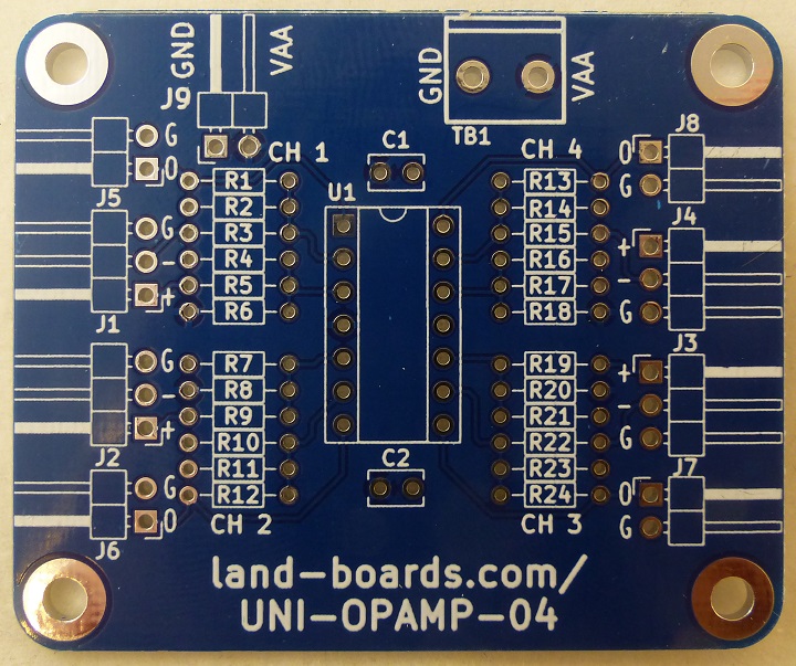
| − | + | [[File:UNI-OPAMP-04_P18586-720px.jpg]] | |
== Features == | == Features == | ||
* Universal OpAmp Board | * Universal OpAmp Board | ||
| − | ** Configurable for typical OpAmp circuits | + | ** Configurable through stuffing options for typical OpAmp circuits |
| − | * 4 Channels | + | ** Through hole parts |
| − | + | ** 14 pin DIP | |
| − | ** [https://www.onsemi.com/pub/Collateral/LM324-D.PDF LM324] | + | ** 1/8 or 1/4W resistors |
| − | + | * 4 Channels, 1 Quad OpAmp | |
| − | + | ** [https://www.onsemi.com/pub/Collateral/LM324-D.PDF LM324], [https://www.microchip.com/wwwproducts/en/MCP6004 MCP6004], [https://www.mouser.com/datasheet/2/294/NJM2060_E-1917248.pdf NJM2060] | |
| − | |||
| − | |||
* Individual input and output headers per channel | * Individual input and output headers per channel | ||
| − | * Terminal block for power | + | * Terminal block or header for power |
* Bypass capacitors | * Bypass capacitors | ||
* 59X49mm form factor | * 59X49mm form factor | ||
* (4) 4-40 mounting holes | * (4) 4-40 mounting holes | ||
| + | |||
| + | === Typical OpAmps=== | ||
| + | |||
| + | {| class="wikitable" | ||
| + | ! Part | ||
| + | ! LM324 | ||
| + | ! MCP6004 | ||
| + | ! NJM2060 | ||
| + | |- | ||
| + | | Operating Voltage | ||
| + | | 3 to 30V | ||
| + | | 1.8V to 6V | ||
| + | | +/-4 to +/-18V | ||
| + | |- | ||
| + | | GBW Product | ||
| + | | 1.2 MHz | ||
| + | | 1 MHz | ||
| + | | 10 MHz | ||
| + | |- | ||
| + | | Output Current (mA) | ||
| + | | 10mA | ||
| + | | 23mA | ||
| + | | 25mA | ||
| + | |- | ||
| + | | Offset Voltage (max) | ||
| + | | 7mV | ||
| + | | 4.5mV | ||
| + | | 6mV | ||
| + | |- | ||
| + | |} | ||
== Connectors == | == Connectors == | ||
| Line 59: | Line 87: | ||
* The resistor mapping from the first channel on the schematic to the other channels are as follows. | * The resistor mapping from the first channel on the schematic to the other channels are as follows. | ||
| − | === | + | === Resistor Stuffing by Channel === |
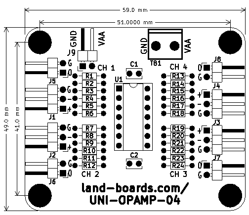
[[FILE:UNI-OPAMP-04 CAD Rev1.PNG]] | [[FILE:UNI-OPAMP-04 CAD Rev1.PNG]] | ||
| Line 108: | Line 136: | ||
== Reference Designs == | == Reference Designs == | ||
| − | * Reference drawings are from [https://www.ti.com/lit/an/snla140c/snla140c.pdf TI Ap Note 31] | + | * Reference drawings are from [https://www.ti.com/lit/an/snla140c/snla140c.pdf TI Ap Note 31 - Op Amp Circuit Collection] |
* Reference designators are for channel 1 | * Reference designators are for channel 1 | ||
** See resistor values table (above) [http://land-boards.com/UNI-OPAMP-08/UNI-OPAMP-08_Schematic.pdf schematic] for other channels | ** See resistor values table (above) [http://land-boards.com/UNI-OPAMP-08/UNI-OPAMP-08_Schematic.pdf schematic] for other channels | ||
| Line 114: | Line 142: | ||
=== Differential Amplifier === | === Differential Amplifier === | ||
| − | ==== Differential Amplifier - Reference Design ==== | + | ==== Differential Amplifier - Reference Design (AN31) ==== |
[[File:Ap31-OpAmp-DiffAmp.PNG]] | [[File:Ap31-OpAmp-DiffAmp.PNG]] | ||
| Line 124: | Line 152: | ||
=== Current to Voltage Converter === | === Current to Voltage Converter === | ||
| − | ==== Current to Voltage Converter - Reference Design | + | ==== Current to Voltage Converter - Reference Design (AN31) ==== |
[[File:Ap31-OpAmp-Curr2Volts.PNG]] | [[File:Ap31-OpAmp-Curr2Volts.PNG]] | ||
| − | ==== Voltage | + | ==== Current to Voltage Stuffing Options ==== |
[[File:OpAMP-sch - Curr2Volts.PNG]] | [[File:OpAMP-sch - Curr2Volts.PNG]] | ||
| Line 134: | Line 162: | ||
=== Inverting Amplifier === | === Inverting Amplifier === | ||
| − | ==== Inverting Amplifier - Reference Design ==== | + | ==== Inverting Amplifier - Reference Design (AN31) ==== |
[[File:Ap31-OpAmp-InvAmp.PNG]] | [[File:Ap31-OpAmp-InvAmp.PNG]] | ||
| Line 144: | Line 172: | ||
=== Non-inverting Amplifier === | === Non-inverting Amplifier === | ||
| − | ==== Non-inverting Amplifier - Reference Design | + | ==== Non-inverting Amplifier - Reference Design (AN31) ==== |
[[File:Ap31-OpAmp-NonInvAmp.PNG]] | [[File:Ap31-OpAmp-NonInvAmp.PNG]] | ||
| Line 154: | Line 182: | ||
== Schematic == | == Schematic == | ||
| − | * [http://land-boards.com/UNI-OPAMP- | + | * [http://land-boards.com/UNI-OPAMP-04/UNI-OPAMP-04_Rev1_Schematic.pdf Schematic] |
| + | |||
| + | === Single Channel Schematic (Editable) === | ||
| + | |||
| + | [[File:OpAMP-sch-EDITABLE.png]] | ||
| + | |||
| + | === U1 Part A Schematic === | ||
| + | |||
| + | [[file:UNI-UPAMP-04_PartA.PNG]] | ||
| + | |||
| + | === U1 Part B Schematic === | ||
| + | |||
| + | [[file:UNI-UPAMP-04_PartB.PNG]] | ||
| + | |||
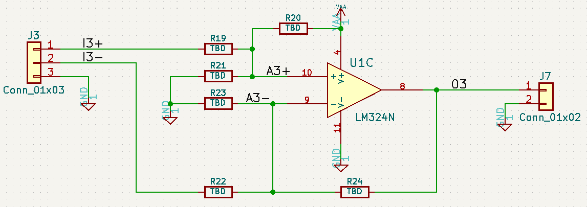
| + | === U1 Part C Schematic === | ||
| + | |||
| + | [[file:UNI-UPAMP-04_PartC.PNG]] | ||
| + | |||
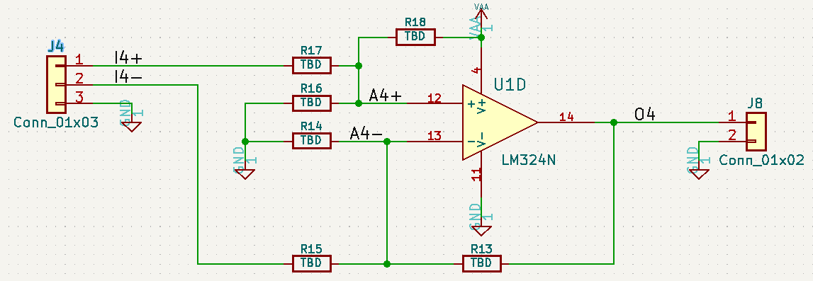
| + | === U1 Part D Schematic === | ||
| + | |||
| + | [[file:UNI-UPAMP-04_PartD.PNG]] | ||
| + | |||
| + | == Test == | ||
| + | |||
| + | === Measure OpAmp Input offset voltages === | ||
| + | |||
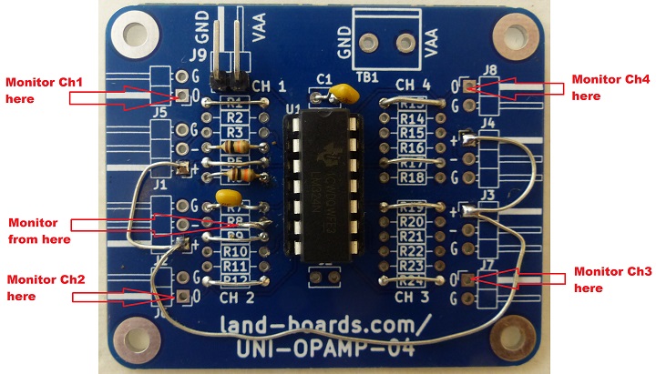
| + | * Configure UNI-OPAMP-04 measure input offset voltages | ||
| + | |||
| + | [[file:UNI-OPAMP-04_P18584-OffsetVoltages_720px.jpg]] | ||
| + | |||
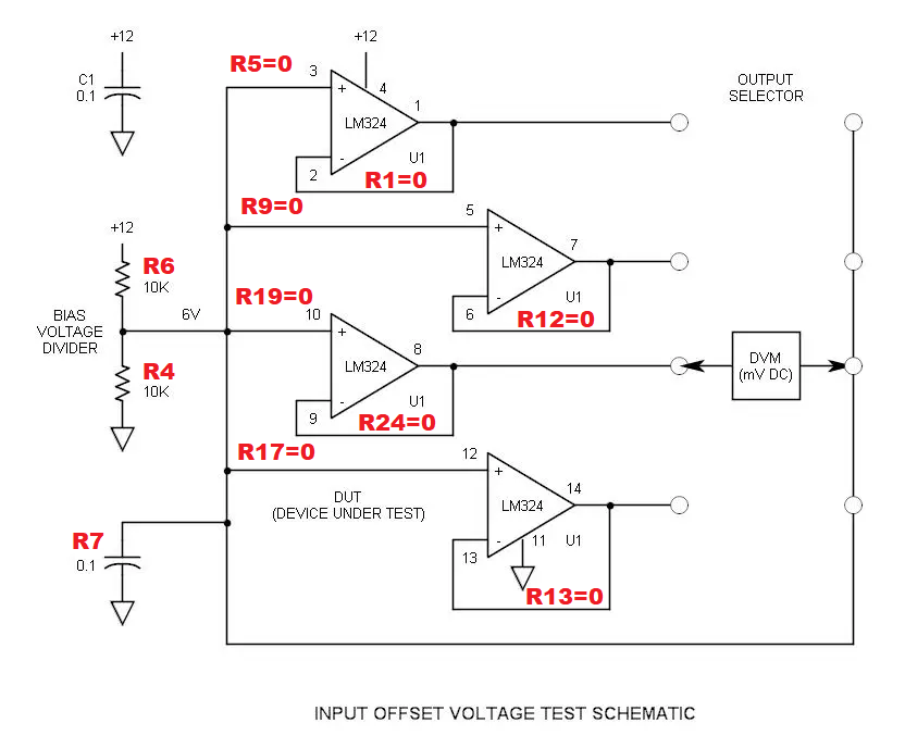
| + | * From [https://www.electroschematics.com/test-op-amps-via-simple-input-offset-voltage-measurement/ Test Op Amps Via Simple Input Offset Voltage Measurement] | ||
| + | * [[Benchtop_Power_Supply_DPS3005|DPS3005 Power Supply]] | ||
| + | ** 0.1A current limit | ||
| + | ** Use built in current meter to measure power supply current | ||
| + | * Measure using DMM Extec EX330 | ||
| + | ** 0.1 mV resolution | ||
| + | * Pick off split voltage at R8 (not power side) | ||
| + | * 12V for LM324NE3, NJM2080D | ||
| + | * 5V for MCP6004-E/IP | ||
| + | * Jumpers between + inputs | ||
| + | |||
| + | [[file:Input-Offset-Voltage-Test-Schematic_Ann.png]] | ||
| + | |||
| + | === Voltage Offset Measurements === | ||
| + | |||
| + | * New parts purchased from Mouser 2022-Aug | ||
| + | * Bought tubes of 10 each | ||
| + | * Picked first part out of each tube | ||
| + | |||
| + | * [https://www.mouser.com/ProductDetail/595-LM324NE3 LM324NE3] | ||
| + | ** Channel A, 0.7mV | ||
| + | ** Channel B, 0.3mV | ||
| + | ** Channel C, 0.5mV | ||
| + | ** Channel D, 0.5mV | ||
| + | ** Vcc = 12V | ||
| + | ** Icc = 1mA | ||
| + | * [https://www.mouser.com/ProductDetail/513-NJM2060D NJM2080D] | ||
| + | ** Channel A, 0.2mV | ||
| + | ** Channel B, 0.4mV | ||
| + | ** Channel C, 0.7mV | ||
| + | ** Channel D, 0.6mV | ||
| + | ** Vcc = 12V | ||
| + | ** Icc = 8mA | ||
| + | * [https://www.mouser.com/ProductDetail/579-MCP6004-E-P MCP6004] | ||
| + | ** Channel A, <0.1mV | ||
| + | ** Channel B, 0.8mV | ||
| + | ** Channel C, 1.3mV | ||
| + | ** Channel D, 1.1mV | ||
| + | ** Vcc = 5V | ||
| + | ** Icc = 1mA | ||
| + | |||
| + | == Mechanicals == | ||
| + | |||
| + | [[file:UNI-OPAMP-04_REV1_MECHS.PNG]] | ||
| + | |||
| + | == Videos == | ||
| + | |||
| + | * [https://www.youtube.com/playlist?list=PLXDK0MeyK4ZgWkzd59wLkir7ZjI7fIsFn IMSAIGuy OpAmp videos playlist] | ||
| + | |||
| + | <video type="youtube">YeNpd-sXaHk</video> | ||
| − | == | + | == Assembly Sheet == |
| − | [[ | + | * [[UNI-OPAMP-04 Rev 1 Assembly Sheet]] |
Latest revision as of 11:26, 22 August 2022
Contents
Features
- Universal OpAmp Board
- Configurable through stuffing options for typical OpAmp circuits
- Through hole parts
- 14 pin DIP
- 1/8 or 1/4W resistors
- 4 Channels, 1 Quad OpAmp
- Individual input and output headers per channel
- Terminal block or header for power
- Bypass capacitors
- 59X49mm form factor
- (4) 4-40 mounting holes
Typical OpAmps
| Part | LM324 | MCP6004 | NJM2060 |
|---|---|---|---|
| Operating Voltage | 3 to 30V | 1.8V to 6V | +/-4 to +/-18V |
| GBW Product | 1.2 MHz | 1 MHz | 10 MHz |
| Output Current (mA) | 10mA | 23mA | 25mA |
| Offset Voltage (max) | 7mV | 4.5mV | 6mV |
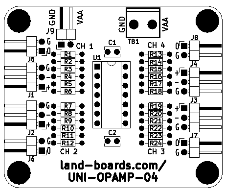
Connectors
J1-J4 - Inputs
- Pinout
- Opamp + input
- Opamp - input
- GND
- J1 - CH 1
- J2 - CH 2
- J3 - CH 3
- J4 - CH 4
J5-J8 - Outputs
- Pinouts
- Opamp Out
- GND
- J5 - CH 1
- J6 - CH 2
- J7 - CH 3
- J8 - CH 4
Configurations
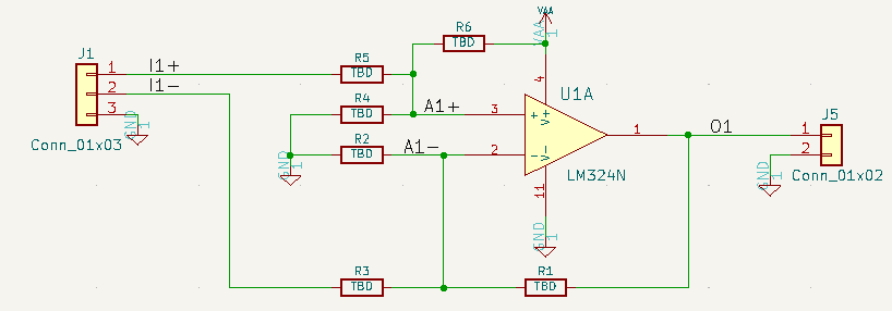
- The reference designs (below) are for the first channel.
- The resistor mapping from the first channel on the schematic to the other channels are as follows.
Resistor Stuffing by Channel
| OpAmp | Ax-/Ix- | Ax+/Ix+ | Ax-/Qx | Ax-/GND | Ax+/GND | Ax+/VCC |
|---|---|---|---|---|---|---|
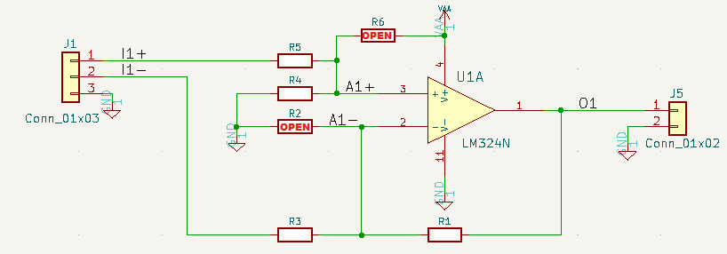
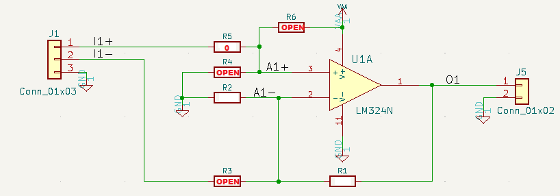
| U1A | R3 | R5 | R1 | R2 | R4 | R6 |
| U1B | R10 | R9 | R12 | R11 | R7 | R8 |
| U1C | R22 | R19 | R24 | R23 | R21 | R20 |
| U1D | R15 | R17 | R13 | R14 | R16 | R18 |
Reference Designs
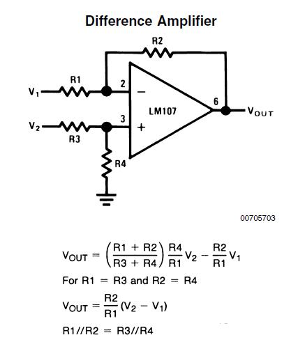
- Reference drawings are from TI Ap Note 31 - Op Amp Circuit Collection
- Reference designators are for channel 1
- See resistor values table (above) schematic for other channels
Differential Amplifier
Differential Amplifier - Reference Design (AN31)
Differential Amplifier Stuffing Options
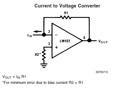
Current to Voltage Converter
Current to Voltage Converter - Reference Design (AN31)
Current to Voltage Stuffing Options
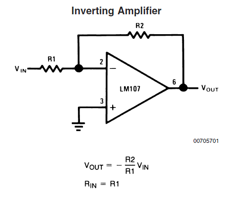
Inverting Amplifier
Inverting Amplifier - Reference Design (AN31)
Inverting Amplifier Stuffing Options
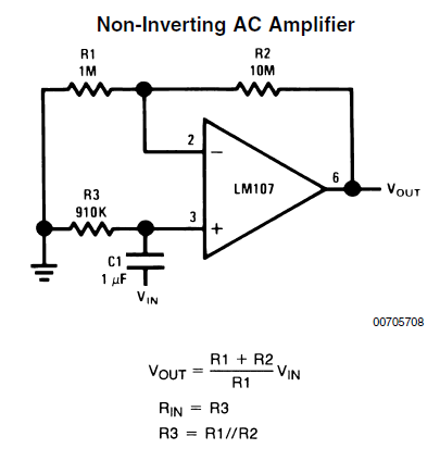
Non-inverting Amplifier
Non-inverting Amplifier - Reference Design (AN31)
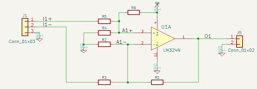
Non-inverting Stuffing Options
Schematic
Single Channel Schematic (Editable)
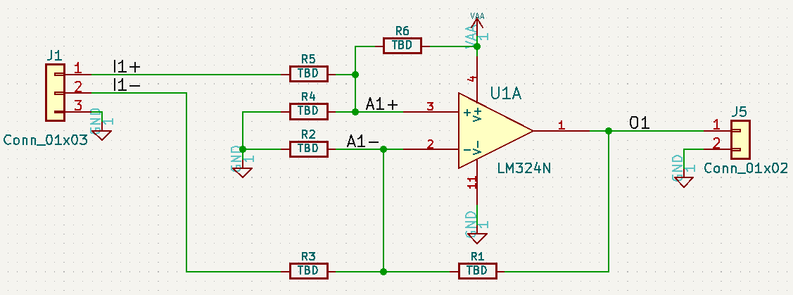
U1 Part A Schematic
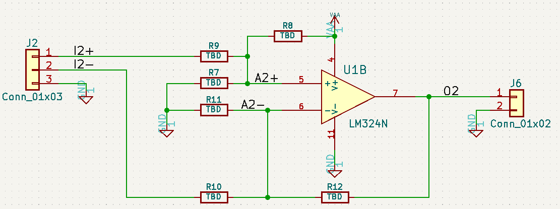
U1 Part B Schematic
U1 Part C Schematic
U1 Part D Schematic
Test
Measure OpAmp Input offset voltages
- Configure UNI-OPAMP-04 measure input offset voltages
- From Test Op Amps Via Simple Input Offset Voltage Measurement
- DPS3005 Power Supply
- 0.1A current limit
- Use built in current meter to measure power supply current
- Measure using DMM Extec EX330
- 0.1 mV resolution
- Pick off split voltage at R8 (not power side)
- 12V for LM324NE3, NJM2080D
- 5V for MCP6004-E/IP
- Jumpers between + inputs
Voltage Offset Measurements
- New parts purchased from Mouser 2022-Aug
- Bought tubes of 10 each
- Picked first part out of each tube
- LM324NE3
- Channel A, 0.7mV
- Channel B, 0.3mV
- Channel C, 0.5mV
- Channel D, 0.5mV
- Vcc = 12V
- Icc = 1mA
- NJM2080D
- Channel A, 0.2mV
- Channel B, 0.4mV
- Channel C, 0.7mV
- Channel D, 0.6mV
- Vcc = 12V
- Icc = 8mA
- MCP6004
- Channel A, <0.1mV
- Channel B, 0.8mV
- Channel C, 1.3mV
- Channel D, 1.1mV
- Vcc = 5V
- Icc = 1mA
Mechanicals
Videos

