Difference between revisions of "ER-ADSR-555-01"
Jump to navigation
Jump to search
Blwikiadmin (talk | contribs) (→Layout) |
Blwikiadmin (talk | contribs) |
||
| Line 128: | Line 128: | ||
[[FILE:ER-ADSR-555-01_FRONT-END.PNG]] | [[FILE:ER-ADSR-555-01_FRONT-END.PNG]] | ||
| + | |||
| + | ==== Layout ==== | ||
| + | |||
| + | [[file:ER-ADSR-555-01_TOP-OF-CAD.PNG]] | ||
==== Debug Decay Noise ==== | ==== Debug Decay Noise ==== | ||
Revision as of 12:14, 30 January 2023
Contents
Eurorack ADSR Module
Features
- 3U tall, 6 HP wide Eurorack module
- Attack-Decay-Sustain-Release ADSR Module
- Takes in Gate signal, generates CV to VCA
- Attack, decay, and release pots control speed
- Attack, decay, and release times can range from 200ms to 16s
- Sustain pot sets the sustain voltage level
- LED dims to level
- 555 Based design
Credits
- Benjie Jiao MiniADSR
- Original was based on Barry Klein design
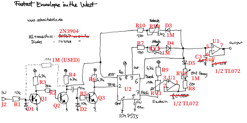
- As built by schmitzbits design - "The Fastest Envelope in the West"
- Benji's build has a three card stack-up and is 4 HP wide
- This card is wider but uses 2 cards
Schematic
Rev 1 Checkout
- Ordered wrong (earlier) version of the board
- Missing 1M decay fix resistor
- Pots are backwards
- Annotated schematic with Rev 1 reference designators
- Drive IN jack with Erica Synths EDU Sequencer
- GATE Out output
- My schematic symbols are Schottky but installed 1N4148 like schmitzbits schemati
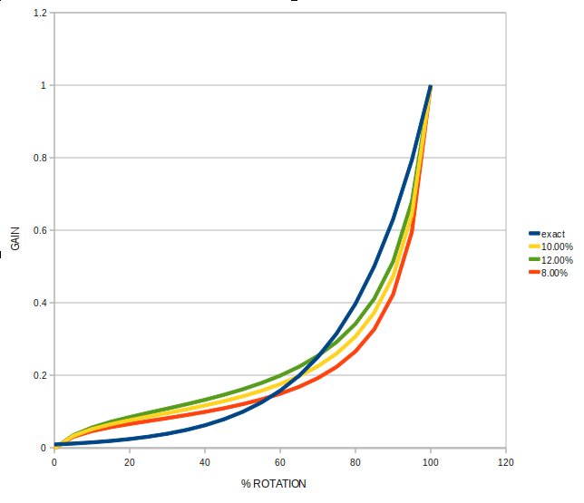
- A, D, R need to be log (Type A) pots
- All of the pots are backwards (rework below)
- A, D, S pots should be CCW for no delay
- S pot should be CW for full output
- ADR series resistors are 220 Ohms but should be 100 Ohms per schmitzbits note
- Attack overshoots
- May need > 100 ohms
- C3 s/b 1 uF for the pots to have a good range
- Updated Pl for above
- Log pot curves
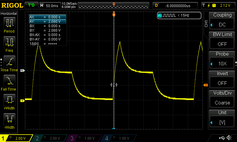
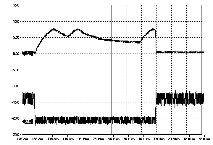
- Scope capture
Schematics
Benjie Jiao - DIY Modular Video
Issues
Rev 2 Issues
- Attack works
- Sustain works
- Release works
- Decay has noise issue
Test Method
- Drive in GATE in for the following
- Measure output
Test Attack
- Set Attack to CCW (min)
- Set Decay pot to CCW (min)
- Set Sustain to CW (max)
- Set Release to CCW (min)
- Adjust Attack
- Front edge rounds over - scope cap
Test Sustain
- Set Attack to CCW (min)
- Set Decay pot to CCW (min)
- Set Sustain to CW (max)
- Set Release to CCW (min)
- Adjust Sustain pot
- Level goes from 0 (CCW) to max (CW)
Test Release
- Set Attack to CCW (min)
- Set Decay pot to CCW (min)
- Set Sustain to CW (max)
- Set Release to CCW (min)
- Adjust Release pot
- Back edge rounds down- scope cap
Test Decay
- Set Attack to just above CCW (8 0-clock) - just a bit of round over on output
- Set Decay pot to CCW (min)
- Set Sustain to just below mid (10-11 o'clock)
- Set Release to CCW (min)
- Release pot set to min (CCW)
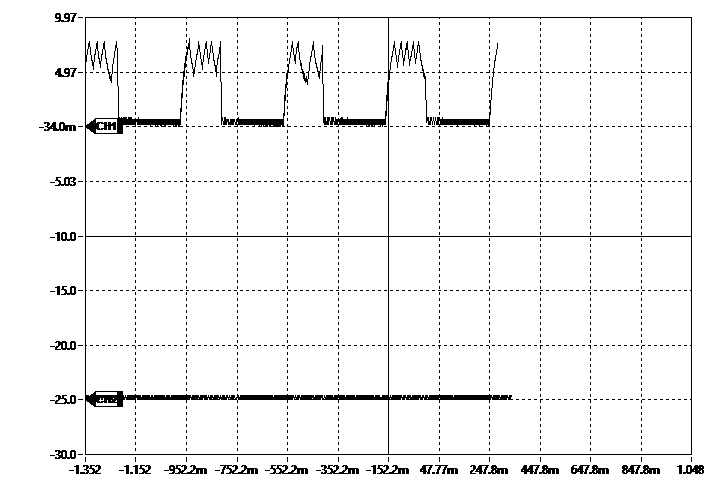
- Adjusting Decay pot near min (CCW) shows noise issue
- Decay starts drop but bounces back up
Schematic of front end
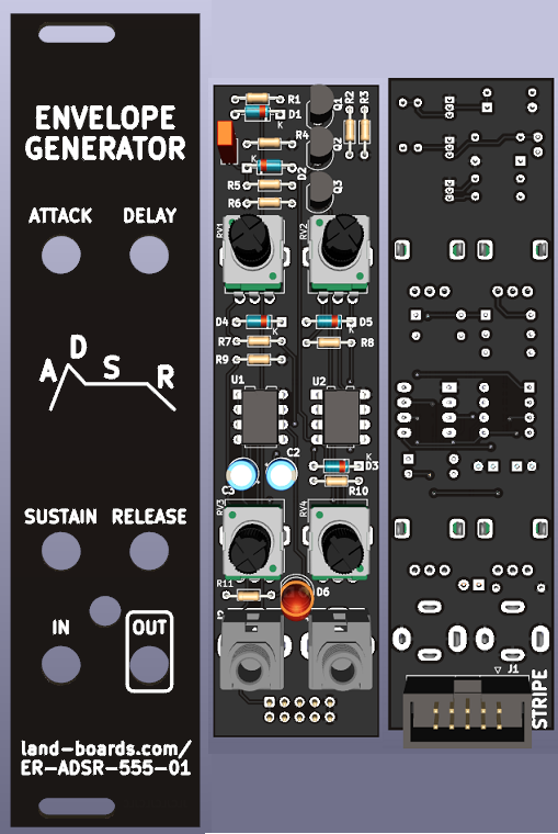
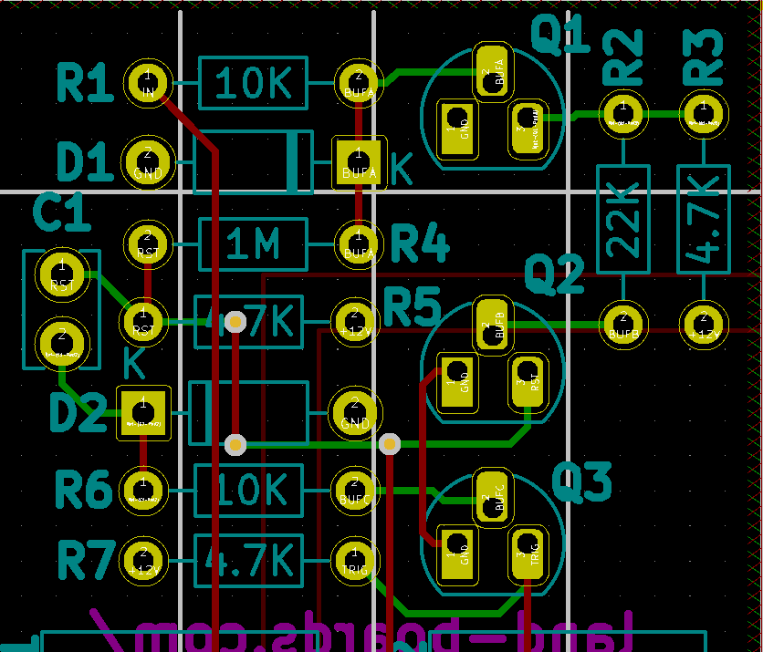
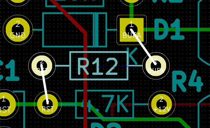
Layout
Debug Decay Noise
- Goal - find Decay Noise mitigation strategy
- Card is sensitive to Eurorack Switching Power Supply noise
- This issue is also present on Rev 1 cards with noise power supply
- Issue did not present for prior testing since rack was lightly loaded at the time
- This issue is also present on Rev 1 cards with noise power supply
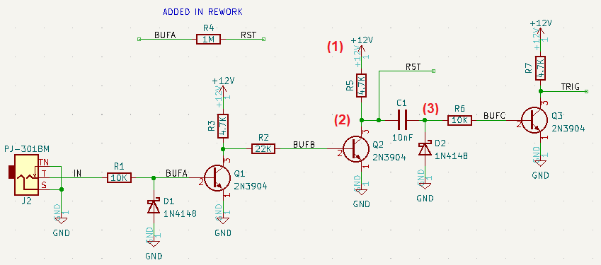
- Tracing noise path (1)-(3) in schematic below
- (1) +12V Vcc noise
- (2) Q2 is "Off", noise through R5 couples through C5
- (3) to Q3 to TRIG
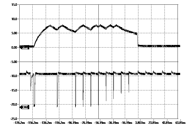
- TRIG (bottom) measured at R7
- Voltage from R2 into Q2 base looks OK
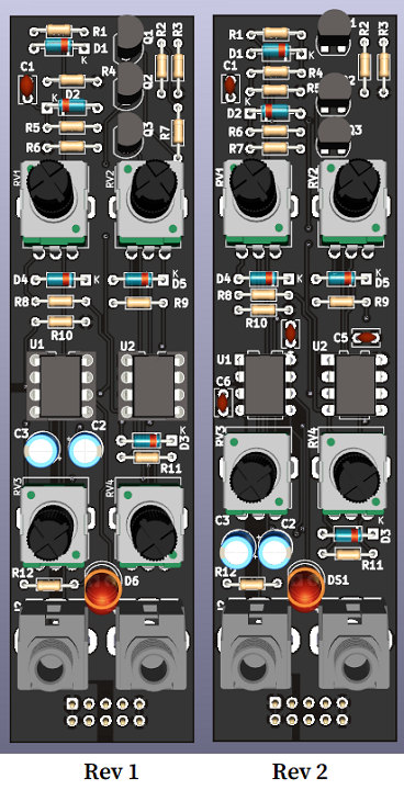
Rev 2 Changes
- Fixed pot ends (swapped ends)
- Added 1M decay resistor "fix" (dashed lines on Schmitz schematic)
- Moved up S, R pots to space them up from jacks
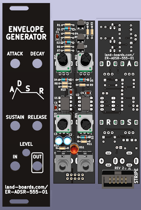
- Updated controls card and front panel
- Added LEVEL legend to front panel silkscreen
- Re-sequenced reference designators
- Change transistor footprints to offset pins/re-oriented
- Better spacing between parts in upper left of controls card
- Added power supply bypass caps (1 per power pin)
- Added URL, Rev 2 marking to rear of card
Rev 1 Issues
- Silkscreen has "DELAY" should be "DECAY"
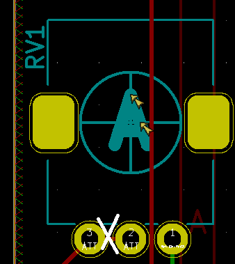
- A, D, S, R pots ends are all backwards
- A, D, R pots should be Type A, 1M Ohms (log pots)
Cuts
- Perform cuts before installing parts on card
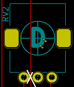
- Cut at RV1 (pins 2-3) top side
- Cut at RV2 (pins 2-3) bottom side
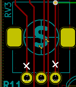
- Cuts at RV3 (pins 1, 3) top side
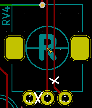
- Cuts at RV4 (pins 2-3 and pin 1)
Change Pot Series Resistor Values
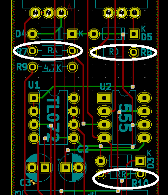
- 220 Ohms on A, D, R pots s/b 100 Ohms (PL below is updated already for this)
- Change R7 to 100 Ohms (A pot)
- Change R8 to 100 Ohms (D pot)
- Change R10 to 100 Ohms (R pot)
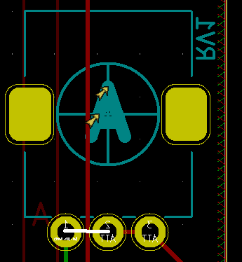
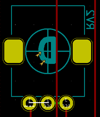
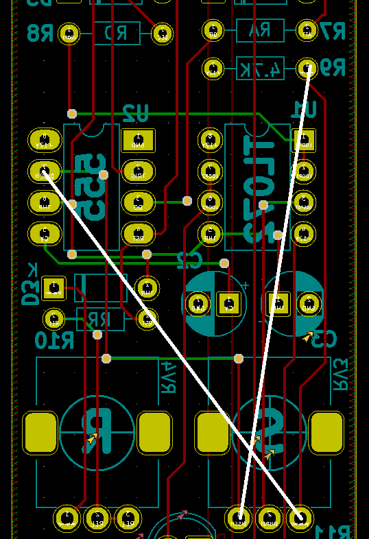
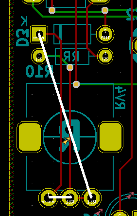
Add wires
- Add wires to rear of card
- Mirrored images below (back side)
- Add wire RV1-2 to RV1-1 (back side view)
- Add wire RV2-2 to RV2-1 (back side view)
- Add wire R9 left side to Sustain pot, RV3-1
- Add wire U2-7 to Sustain pot, RV3-3
- Add wire D3-K to RV4-3 (back side view)
- Add wire RV4-1 to RV4-2 (back side view)
Add Release Resistor
- Add 1M resistor top side of card


