Difference between revisions of "OptoIn8-I2C"
Jump to navigation
Jump to search
Blwikiadmin (talk | contribs) |
Blwikiadmin (talk | contribs) |
||
| (35 intermediate revisions by the same user not shown) | |||
| Line 6: | Line 6: | ||
* Eight optically-isolated input channels on card | * Eight optically-isolated input channels on card | ||
| − | ** (8) 4N25 optoisolators | + | ** (8) 4N25 optoisolators (20% CTR) |
| + | ** 330 ohm series resistor | ||
| + | ** 3.3V or 5V input | ||
| + | ** High input voltage range by either replacing 1/4W R1-R8 resistors or adding additional external resistor | ||
* I2C host interface | * I2C host interface | ||
** MCP23008 I2C Parallel I/O | ** MCP23008 I2C Parallel I/O | ||
** Two Wire interface | ** Two Wire interface | ||
** 100/400 KHZ operation | ** 100/400 KHZ operation | ||
| − | + | ** Jumper selectable I2C SDA/SCL terminators | |
| − | ** Jumper selectable terminators | ||
** 3-bit address (Jumper selectable) - Up to 8 boards | ** 3-bit address (Jumper selectable) - Up to 8 boards | ||
** Single 4-pin host interface connector (Ground, Power, Clock, Data) | ** Single 4-pin host interface connector (Ground, Power, Clock, Data) | ||
| − | * 24LC024 [[ | + | * [https://www.mouser.com/ProductDetail/579-24LC024-P 24LC024] [[Open_Data_Acquisition_System#Personality_EEPROM|ODAS Personality EEPROM]] |
| − | * 3.3V or 5V operation | + | ** pid = 4 |
| + | * 3.3V or 5V Host operation | ||
* Compatible with Arduino, Raspberry Pi, BeagleBone Black | * Compatible with Arduino, Raspberry Pi, BeagleBone Black | ||
| − | * DB-25 connector for rugged uses | + | * DB-25 male Opto input connector for rugged uses |
* 95x95mm form factor | * 95x95mm form factor | ||
* (4) 6-32 mounting holes - one on each corner | * (4) 6-32 mounting holes - one on each corner | ||
| − | === MCP23008 Block Diagram | + | == Opto Inputs - Operation Voltages == |
| + | |||
| + | [[file:OptoIn_Channel.PNG]] | ||
| + | |||
| + | * Typical Opto inputs can be either 3.3V or 5V | ||
| + | ** Higher opto input voltages can be achieved | ||
| + | *** Either replace R1-R8 with higher value resistors or, | ||
| + | *** Adding external input scaling resistors, R1-R8 | ||
| + | *** Factory installed value for R1-R8 is 330 Ohms | ||
| + | |||
| + | === 3.3V Opto Inputs === | ||
| + | |||
| + | * Vin = 3.3V | ||
| + | * V(LED) = 1.2V | ||
| + | * Voltage drop across series resistors (R1-R8) = 2.1V | ||
| + | * Series resistor = 330 Ohms | ||
| + | * Input current = 6.36 mA | ||
| + | * Current transfer ratio (4N25) = 20% (0.2) | ||
| + | * Opto output current (max) 1.2 mA | ||
| + | * Opto out pullup resistor = 4.7K | ||
| + | * Opto Out Voltage depends on Power Supply used for card | ||
| + | ** With 3.3V power supply on card | ||
| + | *** 3.3V/4.7K = 0.7 mA | ||
| + | ** With 5V power supply on card | ||
| + | *** 5/4.7K = 1 mA | ||
| + | *** Sufficient current margin | ||
| + | |||
| + | === 5V Opto Inputs === | ||
| + | |||
| + | * Vin = 5V | ||
| + | * V(LED) = 1.2V | ||
| + | * Voltage drop across series resistors (R1-R8) = 3.8V | ||
| + | * Series resistor = 330 Ohms | ||
| + | * Input current = 11.5 mA | ||
| + | * Current transfer ratio (4N25) = 20% (0.2) | ||
| + | * Opto output current (max) 2.3 mA | ||
| + | * Opto out pullup resistor = 4.7K | ||
| + | * Opto Out Voltage depends on Power Supply used for card | ||
| + | ** With 3.3V power supply on card | ||
| + | *** 3.3V/4.7K = 0.7 mA | ||
| + | ** With 5V power supply on card | ||
| + | *** 5/4.7K = 1 mA | ||
| + | *** Sufficient current margin | ||
| + | |||
| + | == MCP23008 Block Diagram == | ||
[[File:MCP23008-Blk-Dia.PNG]] | [[File:MCP23008-Blk-Dia.PNG]] | ||
| Line 44: | Line 91: | ||
=== J1 - Power === | === J1 - Power === | ||
| − | |||
| − | |||
* Optional power input | * Optional power input | ||
* Can be unused if power is provided via the I2C connectors | * Can be unused if power is provided via the I2C connectors | ||
| + | |||
| + | [[File:OptoIn8-X2-J1.png]] | ||
# GND | # GND | ||
| Line 55: | Line 102: | ||
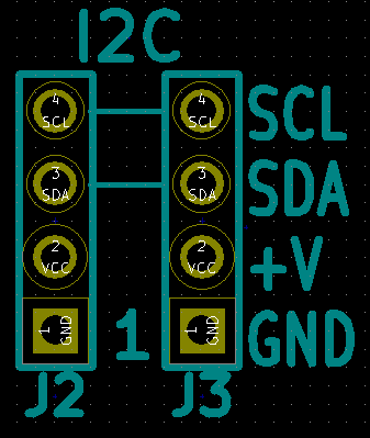
=== J2-J3 - I2C === | === J2-J3 - I2C === | ||
| − | |||
| − | |||
* Daisy Chain connectors | * Daisy Chain connectors | ||
* 2nd connector can be ignored | * 2nd connector can be ignored | ||
| + | |||
| + | [[File:OptoIn8-X2-J2-J3.png]] | ||
# GND | # GND | ||
| Line 67: | Line 114: | ||
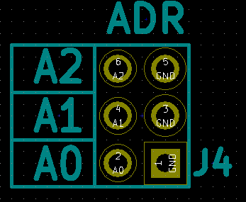
=== J4 - I2C Address Select === | === J4 - I2C Address Select === | ||
| + | |||
| + | * I2C Slave Address offset | ||
| + | * Card base address 0x20 | ||
| + | * Install jumper for Ax = 0 | ||
| + | * Do not install jumper for Ax = 1 | ||
| + | * Factory default is all 3 installed 0x20 | ||
[[File:OptoIn8-X2-J4.png]] | [[File:OptoIn8-X2-J4.png]] | ||
| − | |||
<pre> | <pre> | ||
5-6 = A0 | 5-6 = A0 | ||
| Line 78: | Line 130: | ||
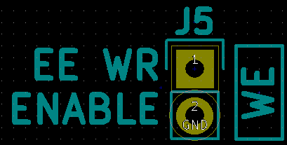
=== J5 - EEPROM Write Enable/Write Protect Jumper === | === J5 - EEPROM Write Enable/Write Protect Jumper === | ||
| + | |||
| + | * Install = Allow EEPROM writes | ||
| + | * Removed = Do not allow writes to EEPROM | ||
[[File:OptoIn8-X2-J5.png]] | [[File:OptoIn8-X2-J5.png]] | ||
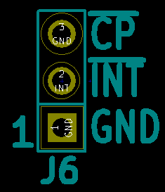
| − | + | === J6 - Card Present/Interrupt === | |
| − | |||
| − | + | * Interrupt out | |
| + | * Card present signal - pulled low on the card | ||
| + | * Neither are required for typical uses | ||
[[File:OptoIn8-X2-J6.png]] | [[File:OptoIn8-X2-J6.png]] | ||
| Line 96: | Line 152: | ||
[[file:OptoIn8-X2-J7.png]] | [[file:OptoIn8-X2-J7.png]] | ||
| − | Install shunts to terminate lines. | + | * Install shunts to terminate I2C lines to Vcc via 2.2K ohm terminators |
| + | * There has to be one set of terminators somewhere on the I2C bus | ||
| + | |||
<pre> | <pre> | ||
3-4 = SDA Terminator | 3-4 = SDA Terminator | ||
| Line 110: | Line 168: | ||
[[File:Db25M.gif]] | [[File:Db25M.gif]] | ||
| − | OptoIn8-X2-J8-fixed.png]]] | + | [[File:OptoIn8-X2-J8-fixed.png]]] |
DB-25 | DB-25 | ||
| Line 129: | Line 187: | ||
25 N/C | 25 N/C | ||
</pre> | </pre> | ||
| − | |||
| − | |||
| − | |||
| − | |||
== Design Validation/First Article Test == | == Design Validation/First Article Test == | ||
| Line 190: | Line 244: | ||
=== EEPROM Test === | === EEPROM Test === | ||
| − | * Code to write to the EEPROM | + | * Code to read/write to the EEPROM |
| − | + | * Select E for EEPROM | |
| − | + | * R to read, W to write | |
| − | |||
| − | |||
| − | |||
| − | |||
| − | |||
| − | |||
| − | |||
| − | |||
| − | * | ||
<pre> | <pre> | ||
| − | + | R=Read EEPROM, W=Write EEPROM, X=Exit Menu | |
| − | + | Reading EEPROM | |
| − | + | Family = ODAS | |
| − | Product=OptoIn8-I2C | + | Company = land-boards.com |
| + | Product = OptoIn8-I2C | ||
| + | eepromAccessMenu() - Finished reading EEPROM | ||
</pre> | </pre> | ||
== Factory Acceptance Test == | == Factory Acceptance Test == | ||
| + | * Unit Under Test (UUT) | ||
* Runs on [[Open Data Acquisition System]] | * Runs on [[Open Data Acquisition System]] | ||
| − | * The Test Station has an internal DIGIO32 card | + | * I2C cable from [[Open Data Acquisition System]] to I2C connector on the UUT |
| − | * Cable from UUT connector to the DIGIO32 card in the Test Station | + | * The Test Station has an internal DIGIO32 card |
| − | * The DIGIO32 internal to the Test Station is set to all outputs | + | * Cable from UUT connector to the DIGIO32 card in the Test Station |
| + | ** [[DB37RIBBON]] male card | ||
| + | ** [[DB25RIBBON]] female card | ||
| + | ** Ribbon cable 37:25 | ||
| + | * The DIGIO32 internal to the Test Station is set to all outputs | ||
* Put out 8 bit test vector on DIGIO32 pins | * Put out 8 bit test vector on DIGIO32 pins | ||
| − | ** D0 is LED1+ | + | ** D0 is LED1+ ... D7 is LED8+ |
| − | ** D8 is LED1- | + | ** D8 is LED1- ... D15 is LED8- |
| − | * To turn on LED1, set D0 High and D8 Low | + | * To turn on LED1, set D0-D7 High and D8-D15 Low |
* Looks at the returned values on the OptoIn8-I2C | * Looks at the returned values on the OptoIn8-I2C | ||
* The OptoIn8-I2C cards that is the UUT is set up to all inputs. | * The OptoIn8-I2C cards that is the UUT is set up to all inputs. | ||
| − | * USB running puTTY | + | * USB-C connection to PC running [https://www.chiark.greenend.org.uk/~sgtatham/putty/ puTTY] |
** 9600 baud | ** 9600 baud | ||
* Menu driven | * Menu driven | ||
| − | * Auto- | + | |
| + | === EEPROM Setup === | ||
| + | |||
| + | * Auto-detects card if test has been run before | ||
<pre> | <pre> | ||
| Line 248: | Line 303: | ||
Select board > | Select board > | ||
</pre> | </pre> | ||
| − | * Select board | + | * Select board 3 |
<pre> | <pre> | ||
Select board > 3 [OptoIn8-I2C Card] | Select board > 3 [OptoIn8-I2C Card] | ||
| Line 259: | Line 314: | ||
Checking EEPROM for board type...Detected OptoIn8-I2C board | Checking EEPROM for board type...Detected OptoIn8-I2C board | ||
</pre> | </pre> | ||
| + | |||
| + | === Run Test === | ||
| + | |||
* Test 'T' | * Test 'T' | ||
<pre> | <pre> | ||
| Line 286: | Line 344: | ||
OptoIn8-I2C Rev X1 | OptoIn8-I2C Rev X1 | ||
| + | |||
| + | == Assembly Sheet == | ||
| + | |||
| + | [[OptoIn8-I2C Assembly Sheet]] | ||
Latest revision as of 17:55, 12 June 2023
Contents
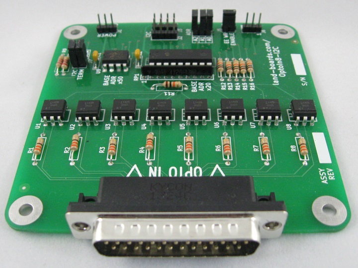
Features
- Eight optically-isolated input channels on card
- (8) 4N25 optoisolators (20% CTR)
- 330 ohm series resistor
- 3.3V or 5V input
- High input voltage range by either replacing 1/4W R1-R8 resistors or adding additional external resistor
- I2C host interface
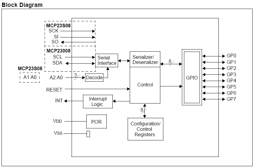
- MCP23008 I2C Parallel I/O
- Two Wire interface
- 100/400 KHZ operation
- Jumper selectable I2C SDA/SCL terminators
- 3-bit address (Jumper selectable) - Up to 8 boards
- Single 4-pin host interface connector (Ground, Power, Clock, Data)
- 24LC024 ODAS Personality EEPROM
- pid = 4
- 3.3V or 5V Host operation
- Compatible with Arduino, Raspberry Pi, BeagleBone Black
- DB-25 male Opto input connector for rugged uses
- 95x95mm form factor
- (4) 6-32 mounting holes - one on each corner
Opto Inputs - Operation Voltages
- Typical Opto inputs can be either 3.3V or 5V
- Higher opto input voltages can be achieved
- Either replace R1-R8 with higher value resistors or,
- Adding external input scaling resistors, R1-R8
- Factory installed value for R1-R8 is 330 Ohms
- Higher opto input voltages can be achieved
3.3V Opto Inputs
- Vin = 3.3V
- V(LED) = 1.2V
- Voltage drop across series resistors (R1-R8) = 2.1V
- Series resistor = 330 Ohms
- Input current = 6.36 mA
- Current transfer ratio (4N25) = 20% (0.2)
- Opto output current (max) 1.2 mA
- Opto out pullup resistor = 4.7K
- Opto Out Voltage depends on Power Supply used for card
- With 3.3V power supply on card
- 3.3V/4.7K = 0.7 mA
- With 5V power supply on card
- 5/4.7K = 1 mA
- Sufficient current margin
- With 3.3V power supply on card
5V Opto Inputs
- Vin = 5V
- V(LED) = 1.2V
- Voltage drop across series resistors (R1-R8) = 3.8V
- Series resistor = 330 Ohms
- Input current = 11.5 mA
- Current transfer ratio (4N25) = 20% (0.2)
- Opto output current (max) 2.3 mA
- Opto out pullup resistor = 4.7K
- Opto Out Voltage depends on Power Supply used for card
- With 3.3V power supply on card
- 3.3V/4.7K = 0.7 mA
- With 5V power supply on card
- 5/4.7K = 1 mA
- Sufficient current margin
- With 3.3V power supply on card
MCP23008 Block Diagram
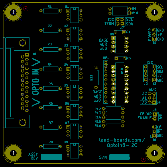
Layout
Power
Vin		5	V	12
Vdiode		1.7	V	1.7
Vres		3.3	V	10.3
I		0.01	A	0.01
PwrRes		0.033	W	0.103
ResRatedPwr	0.25	W	0.25
Derated		13.2	%	41.2
Connectors
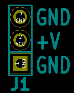
J1 - Power
- Optional power input
- Can be unused if power is provided via the I2C connectors
- GND
- VCC
- GND
J2-J3 - I2C
- Daisy Chain connectors
- 2nd connector can be ignored
- GND
- VCC
- SDA
- SCL
J4 - I2C Address Select
- I2C Slave Address offset
- Card base address 0x20
- Install jumper for Ax = 0
- Do not install jumper for Ax = 1
- Factory default is all 3 installed 0x20
5-6 = A0
3-4 = A1
1-2 = A2
J5 - EEPROM Write Enable/Write Protect Jumper
- Install = Allow EEPROM writes
- Removed = Do not allow writes to EEPROM
J6 - Card Present/Interrupt
- Interrupt out
- Card present signal - pulled low on the card
- Neither are required for typical uses
- GND
- INT
- CP - Card present (pulled low)
J7 - I2C Terminators Jumpers
- Install shunts to terminate I2C lines to Vcc via 2.2K ohm terminators
- There has to be one set of terminators somewhere on the I2C bus
3-4 = SDA Terminator
1-2 = SCK Terminator
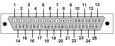
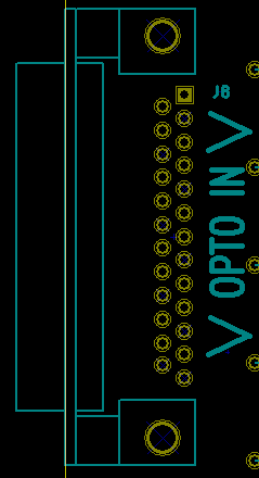
J8 - I/O connector
OptoIn8-Connector
DB-25
Pin	Descr		Pin	Descr
1	CH1-IN+		14	CH1-IN-
15	CH2-IN+		3	CH2-IN-
4	CH3-IN+		17	CH3-IN-
18	CH4-IN+		6	CH4-IN-
7	CH5-IN+		20	CH5-IN-
21	CH6-IN+		9	CH6-IN-
10	CH7-IN+		23	CH7-IN-
24	CH8-IN+		12	CH8-IN-
2	N/C		5	N/C
8	N/C		11	N/C
13	N/C		16	N/C
19	N/C		22	N/C
25	N/C
Design Validation/First Article Test
Read Single Opto Input Channel Test
- Test code
- Write out on Arduino D8 line
- D8 is wired to the first Opto channel
- Read back Opto channel
- Result is complement of write data
Wrote HIGH, read back 0
Wrote LOW, read back  1
Read all 8 Channels
8 channel read card
Wrote LOW to channel  1, read back  FF
Wrote HIGH to channel 1, read back  FE
Wrote LOW to channel  2, read back  FF
Wrote HIGH to channel 2, read back  FD
Wrote LOW to channel  3, read back  FF
Wrote HIGH to channel 3, read back  FB
Wrote LOW to channel  4, read back  FF
Wrote HIGH to channel 4, read back  F7
Wrote LOW to channel  5, read back  FF
Wrote HIGH to channel 5, read back  EF
Wrote LOW to channel  6, read back  FF
Wrote HIGH to channel 6, read back  DF
Wrote LOW to channel  7, read back  FF
Wrote HIGH to channel 7, read back  BF
Wrote LOW to channel  8, read back  FF
Wrote HIGH to channel 8, read back  7F
Wrote LOW to channel  1, read back  FF
Wrote HIGH to channel 1, read back  FE
Wrote LOW to channel  2, read back  FF
Wrote HIGH to channel 2, read back  FD
Wrote LOW to channel  3, read back  FF
Wrote HIGH to channel 3, read back  FB
Wrote LOW to channel  4, read back  FF
Wrote HIGH to channel 4, read back  F7
Wrote LOW to channel  5, read back  FF
Wrote HIGH to channel 5, read back  EF
Wrote LOW to channel  6, read back  FF
Wrote HIGH to channel 6, read back  DF
Wrote LOW to channel  7, read back  FF
Wrote HIGH to channel 7, read back  BF
Wrote LOW to channel  8, read back  FF
Wrote HIGH to channel 8, read back  7F
Pass/Fail version of the code
EEPROM Test
- Code to read/write to the EEPROM
- Select E for EEPROM
- R to read, W to write
R=Read EEPROM, W=Write EEPROM, X=Exit Menu
Reading EEPROM
Family  = ODAS
Company = land-boards.com
Product = OptoIn8-I2C
eepromAccessMenu() - Finished reading EEPROM
Factory Acceptance Test
- Unit Under Test (UUT)
- Runs on Open Data Acquisition System
- I2C cable from Open Data Acquisition System to I2C connector on the UUT
- The Test Station has an internal DIGIO32 card
- Cable from UUT connector to the DIGIO32 card in the Test Station
- DB37RIBBON male card
- DB25RIBBON female card
- Ribbon cable 37:25
- The DIGIO32 internal to the Test Station is set to all outputs
- Put out 8 bit test vector on DIGIO32 pins
- D0 is LED1+ ... D7 is LED8+
- D8 is LED1- ... D15 is LED8-
- To turn on LED1, set D0-D7 High and D8-D15 Low
- Looks at the returned values on the OptoIn8-I2C
- The OptoIn8-I2C cards that is the UUT is set up to all inputs.
- USB-C connection to PC running puTTY
- 9600 baud
- Menu driven
EEPROM Setup
- Auto-detects card if test has been run before
Checking EEPROM for board type...Detected OptoIn8-I2C board
R=Read EEPROM, W=Write EEPROM, T=Test DIGIOs, L=Loop Test, B=Bounce LEDs
- If the EEPROM has not been programmed (first time for the test to be run)
Checking EEPROM for board type...Company Mismatch
Select the board type
1 - DIGIO16-I2C board
2 - DIGIO-128 board
3 - OptoIn8-I2C board
4 - OptoOut8-I2C board
5 - DIGIO32-I2C board
6 - PROTO16-I2C board
7 - ODAS-PSOC5 board
8 - ODAS-RELAY16 board
9 - TBD board
X - Boards without EEPROMs
Select board >
- Select board 3
Select board > 3 [OptoIn8-I2C Card]
Writing EEPROM
Initializing eep buffer
len of buffer=96
reading block
Family=ODAS
Company=land.boards.com
Checking EEPROM for board type...Detected OptoIn8-I2C board
Run Test
- Test 'T'
R=Read EEPROM, W=Write EEPROM, T=Test DIGIOs, L=Loop Test, B=Bounce LEDs
Loopback Test PASS = 1, FAIL = 0
Revision History
Rev X3 to Rev X4 PWB changes
- Moved the DB-25 mounting holes to center on the connector pins
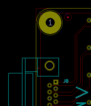
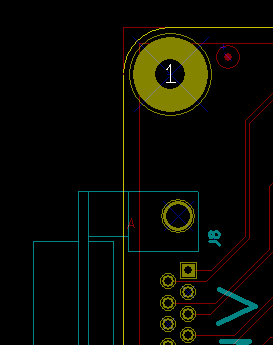
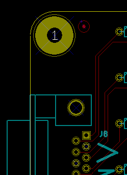
Rev X2 to Rev X3 PWB changes
- Move DB connector (J8) left from X=22.7 mm to X=17 mm
Rev X1
OptoIn8-I2C Rev X1

