Difference between revisions of "LB-65CXX-01"
Jump to navigation
Jump to search
Blwikiadmin (talk | contribs) |
Blwikiadmin (talk | contribs) |
||
| Line 215: | Line 215: | ||
* [[SIMPLE-6502#Software|SIMPLE-6502 Software]] | * [[SIMPLE-6502#Software|SIMPLE-6502 Software]] | ||
| + | * [http://searle.x10host.com/6502/osi_bas.zip Link to Grant's files] | ||
| + | * Source code | ||
| + | ** osi_bas.s <== the Microsoft OSI BASIC and I/O routines SOURCE all in a single file | ||
| + | ** Grant's I/O routines are at the end of it | ||
| + | * Files to allow the source to be assembled on a Windows based machine | ||
| + | ** assemble.bat <== double click to assemble osi_bas.s and link to binary file "osi_bas.bin" | ||
| + | ** This should be exactly 16K | ||
| + | ** osi_bas.cfg <== configuration file for the linker (ensure ORG and entries in this file match if you change any) | ||
| + | ** ca65.exe <== the assembler from the cc65 package. Use this. The new version on the cc65 site crashes! | ||
| + | ** ld65.exe <== linker from the cc65 package | ||
| + | * Output files | ||
| + | ** osi_bas.bin <== the ROM fine in pure binary | ||
| + | ** osi_bas.lst <== Assembly listing file | ||
| + | ** rom.hex <== the ROM fine in standard INTEL-HEX format | ||
| + | * To allow simple re-assembly, extract all files to the same folder | ||
| + | ** Freeware utilities are available to convert the "bin" file to HEX or s19 (etc) - use your internet search tool to find | ||
| + | * All source code, assembler binaries and the HEX dump of the ROM is [http://searle.x10host.com/6502/osi_bas.zip here] | ||
| + | ** It is in standard INTEL-HEX format for uploading to a suitable programmer. | ||
== Mechanicals == | == Mechanicals == | ||
Revision as of 23:46, 11 September 2024
Features
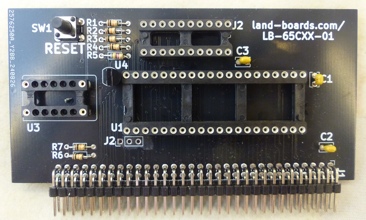
- 65C02 or 65C816 CPU
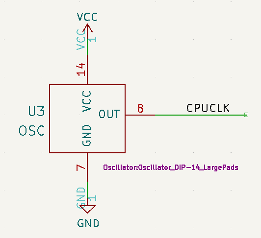
- 2 MHz (typical) Oscillator on card
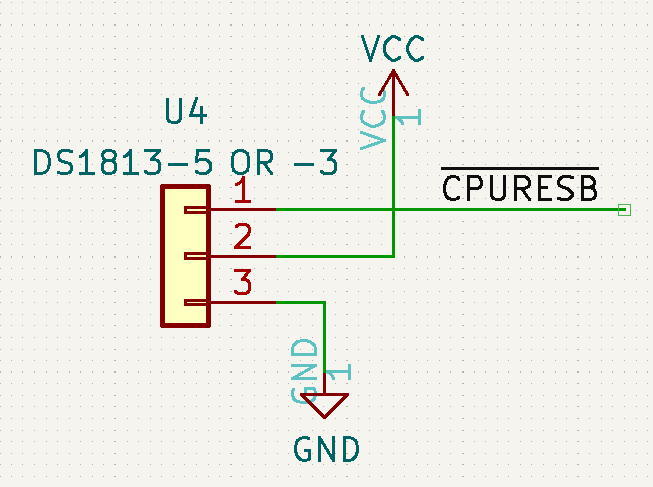
- Reset switch/power monitor
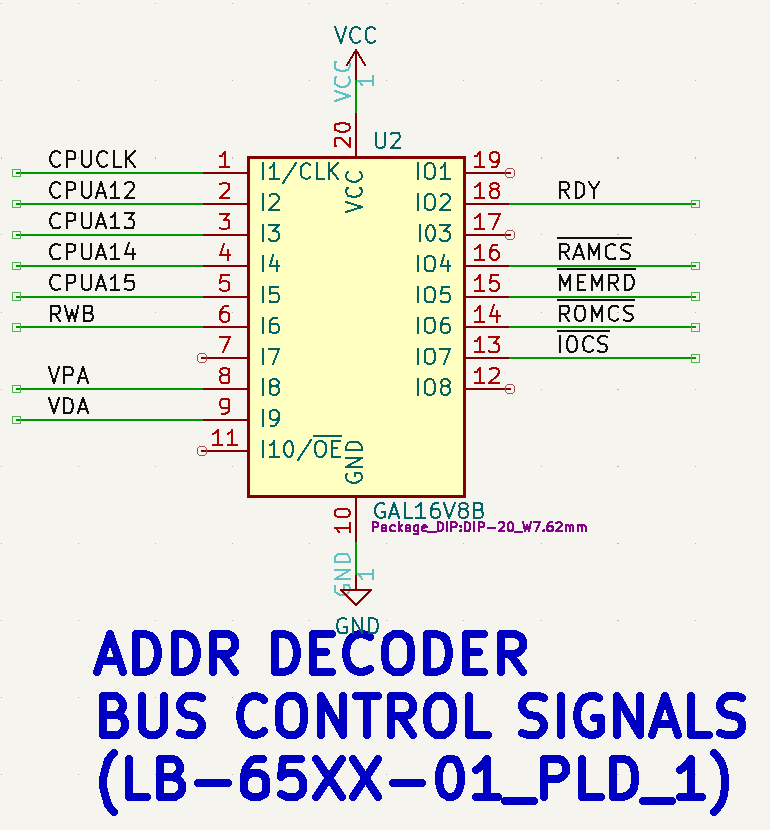
- Address decoder PLD drives RAM/ROM/IO chip selects
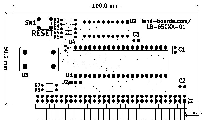
- 100x50mm card
Design
Memory Map
0x0000-0x7FFF - 32KB SRAM
0x8000-0x8FFF - 4KB I/O space
0x9000-0xBFFF - Free space (12 KB SRAM Using 128KB SRAM)
0xC000-0xFFFF - 16KB EPROM space
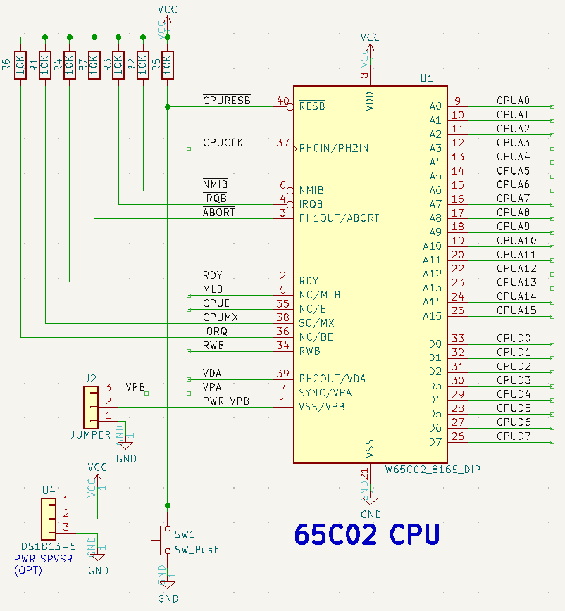
CPU
- 65C02 or 65C816 CPU
- 65C816 requires mods to the PCB (see Checkout notes below) or Rev 2 PCB
- 2 MHz
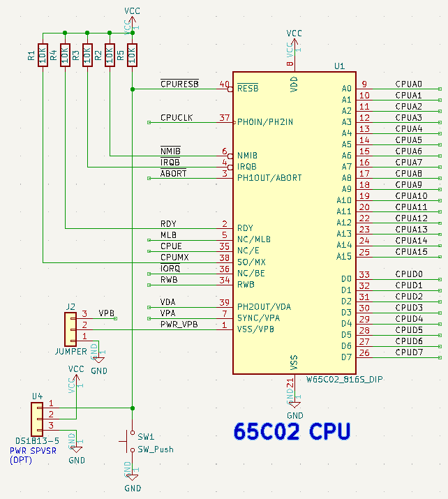
- Install jumper J2:1-2 if CPU is not a WDC 65C02 or WDC 65C816
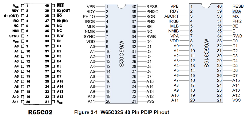
R65C02 vs W65C02 vs W65C816 CPUs
| U1 Pin | U1 Pin Name | Sig Name | Pullup | R65C02 sig | W65C02 sig | W65C816 sig |
|---|---|---|---|---|---|---|
| 1 | VSS/VPB | J2 selects | N | VSS (IN) | VPB (OUT) | VPB (OUT) |
| 3 | PH1OUT/ABORT | ABORT* | REV2 | PH1OUT (OUT) | PH1OUT (OUT) | ABORT (IN) |
| 5 | NC/MLB | MLB | N | NC | MLB (OUT) | MLB (OUT) |
| 7 | SYNC/VPA | VPA | N | SYNC (OUT) | SYNC (OUT) | VPA (OUT) |
| 35 | NC/E | CPUE | N | NC | NC | EM/NAT (OUT) |
| 36 | NC/BE | IORQ* | REV2 | NC | BE (IN) | BE (IN) |
| 37 | PH0IN/PH2IN | CPUCLK | N | PH0IN | PH2IN | PH2IN |
| 38 | SO/MX | CPUMX | REV1/2 | SO* (IN) | SOB (IN) | MX (OUT) |
| 39 | PH2OUT/VDA | VDA | N | PH2OUT (OUT) | PH2OUT (OUT) | VDA (OUT) |
VDA/VPA (65C816)
- VDA/VDA
- 00, Internal operation (invalid address bus)
- 01, Valid Program Address
- 10, Valid Data Address
- 11, Opcode-fetch
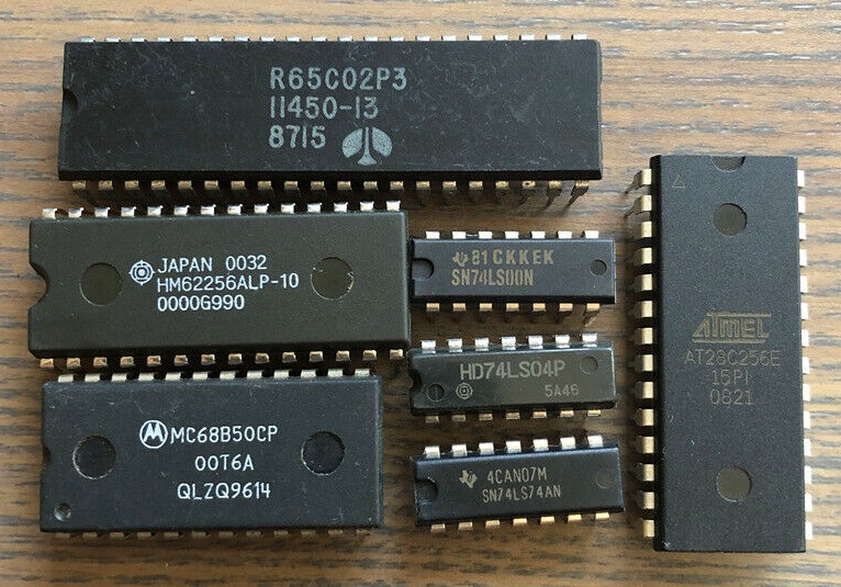
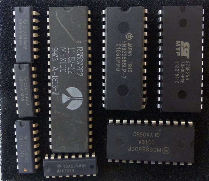
Chip Set
- Picture shows 3 MHz CPU
- Received 2 MHz CPU
- As received:
Oscillator
PLD
- ATF16V8B part
- TL866ii Plus Programmer
PLD Listing
Name       LB-65CXX-01_PLD;
Partno     ATF16V8B;
Date       08/19/24;
Revision   01;
Designer   DOUG G;
Company    LAND BOARDS LLC;
Assembly   LB65CXX01_U2;
Location   Rustbelt, US;
Device     G16V8;

/*
	65C816 Control
*/

/* Control inputs */
PIN    1   = CLK;
PIN    2   = CPUA12;
PIN    3   = CPUA13;
PIN    4   = CPUA14;
PIN    5   = CPUA15;
PIN    6   = CPUREAD;
PIN    8   = VPA;
PIN    9   = VDA;		/* Pin 39, PH2OUT - Enable line */

/* Address Decode and Chip Select outputs */
PIN    13  = !IOCS;
PIN    14  = !ROMCS;
PIN    15  = !MEMRD;
PIN    16  = !RAMCS;
PIN    18  = RDY;

RAMCS = !CPUA15 & VDA								/* 0x0000-0x7FFF (32KB/64KB SRAM)	*/
#        CPUA15 & !CPUA14 & !CPUA13 & CPUA12 & VDA	/* 0x9000-0x9FFF (128KB SRAM)		*/
#        CPUA15 & !CPUA14 &  CPUA13 & VDA;			/* 0xA000-0xBFFF (128KB SRAM)		*/

IOCS = CPUA15 & !CPUA14 & !CPUA13 & !CPUA12 & VDA;	/* 0x8000-0x8FFF (4KB space)		*/

ROMCS = CPUA15 & CPUA14 & CPUREAD & VDA;			/* 0xC000-0xFFFF (16KB space)		*/

MEMRD = !CPUA15 &                              CPUREAD & VDA	/* 0x0000-0x7FFF		*/
#        CPUA15 & !CPUA14 & !CPUA13 & CPUA12 & CPUREAD & VDA	/* 0x9000-0x9FFF		*/
#        CPUA15 & !CPUA14 &  CPUA13 &          CPUREAD & VDA	/* 0xA000-0xBFFF		*/
#        CPUA15 &  CPUA14 &                    CPUREAD & VDA;	/* 0xC000-0xFFFF		*/

/*
RDY = VDA;
*/
Reset Controller
- DS1813-5 Reset Controller
- 5V Power Monitor
- Reset controller
- Reset pushbutton to ground
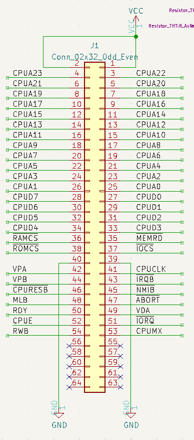
Backplane connector
Software
- SIMPLE-6502 Software
- Link to Grant's files
- Source code
- osi_bas.s <== the Microsoft OSI BASIC and I/O routines SOURCE all in a single file
- Grant's I/O routines are at the end of it
- Files to allow the source to be assembled on a Windows based machine
- assemble.bat <== double click to assemble osi_bas.s and link to binary file "osi_bas.bin"
- This should be exactly 16K
- osi_bas.cfg <== configuration file for the linker (ensure ORG and entries in this file match if you change any)
- ca65.exe <== the assembler from the cc65 package. Use this. The new version on the cc65 site crashes!
- ld65.exe <== linker from the cc65 package
- Output files
- osi_bas.bin <== the ROM fine in pure binary
- osi_bas.lst <== Assembly listing file
- rom.hex <== the ROM fine in standard INTEL-HEX format
- To allow simple re-assembly, extract all files to the same folder
- Freeware utilities are available to convert the "bin" file to HEX or s19 (etc) - use your internet search tool to find
- All source code, assembler binaries and the HEX dump of the ROM is here
- It is in standard INTEL-HEX format for uploading to a suitable programmer.
Mechanicals
Checkout
Rev 2
Rev 2 Checkout
- Install jumper J2:1-2 since CPU is R65C02
- NOP tester - 6502 nop = 0xEA
- Works
Rev 2 Changes
- Add pull-up resistor on ABORT* line (U1-3)
- Add pull-up resistor on BE line (U1-36)
Rev 1
- Install jumper J2:1-2 if CPU is not a WDC 65C02 or WDC 65C816
- If WDC 65C02 or WDC 65C816 is used:
- Add pull-up resistor on ABORT* line (U1-3)
- Add pull-up resistor on BE line (U1-36)
