Difference between revisions of "PDP-11 ON RETRO-EP4CE15"
Jump to navigation
Jump to search
Blwikiadmin (talk | contribs) |
Blwikiadmin (talk | contribs) |
||
| Line 66: | Line 66: | ||
==== RT-11 4.0 (rk05) ==== | ==== RT-11 4.0 (rk05) ==== | ||
| − | * [https://github.com/douggilliland/Retro-Computers/tree/master/PDP-11/Disks/rk05/rt11_v4_rk RT-11 4.0 (rk05)] | + | * [https://github.com/douggilliland/Retro-Computers/tree/master/PDP-11/Disks/rk05/rt11_v4_rk RT-11 4.0 (rk05) Disk Image] |
| + | ** Write to SD card - used Balena Etcher (windows) to write SD card | ||
==== RT-11FB 4.0 (rk05) ==== | ==== RT-11FB 4.0 (rk05) ==== | ||
| Line 74: | Line 75: | ||
==== RT-11 5.4 (rk05) ==== | ==== RT-11 5.4 (rk05) ==== | ||
| − | * [https://github.com/douggilliland/Retro-Computers/tree/master/PDP-11/Disks/rk05/rt11_54_rk RT-11 5.4 (rk05)] | + | * [https://github.com/douggilliland/Retro-Computers/tree/master/PDP-11/Disks/rk05/rt11_54_rk RT-11 5.4 (rk05) Disk Image] |
| + | ** Write to SD card - used Balena Etcher (windows) to write SD card | ||
==== UNIX V7 (rl02) ==== | ==== UNIX V7 (rl02) ==== | ||
| − | * [https://github.com/douggilliland/Retro-Computers/tree/master/PDP-11/Disks/rl02/Unix_v7_rl UNIX V7 (rl02)] | + | * [https://github.com/douggilliland/Retro-Computers/tree/master/PDP-11/Disks/rl02/Unix_v7_rl UNIX V7 (rl02) Disk Image] |
| + | ** Write to SD card - used Balena Etcher (windows) to write SD card | ||
=== PDP-11/70 disks === | === PDP-11/70 disks === | ||
| Line 84: | Line 87: | ||
==== 211BSD (rp06) ==== | ==== 211BSD (rp06) ==== | ||
| − | * [https://github.com/douggilliland/Retro-Computers/tree/master/PDP-11/Disks/rp06/211bsd 211BSD (rp06)] | + | * [https://github.com/douggilliland/Retro-Computers/tree/master/PDP-11/Disks/rp06/211bsd 211BSD (rp06) Disk Image] |
| + | ** Write to SD card - used Balena Etcher (windows) to write SD card | ||
==== RSX-11M PLUS 3.0 (rp06) ==== | ==== RSX-11M PLUS 3.0 (rp06) ==== | ||
| − | * [https://github.com/douggilliland/Retro-Computers/tree/master/PDP-11/Disks/rp06/rsx11mp-30 RSX-11M PLUS 3.0 (rp06)] | + | * [https://github.com/douggilliland/Retro-Computers/tree/master/PDP-11/Disks/rp06/rsx11mp-30 RSX-11M PLUS 3.0 (rp06) Disk Image] |
| + | ** Write to SD card - used Balena Etcher (windows) to write SD card | ||
== Other Disk Images == | == Other Disk Images == | ||
Revision as of 15:21, 1 May 2022
Contents
- 1 Overview
- 2 PDP2011 FPGA Builds
- 3 Hardware
- 4 Disks (SD card images) that work with PDP2011 build
- 5 Other Disk Images
- 6 Other PDP2011 Builds
- 7 Documentation
- 8 PDP-11 Front Panel
- 9 Connectors on RETROEP4-CE15 Card
- 10 FPGA Resources
- 11 External Resources
- 12 Programming the FPGA EEPROM (5CEFA2F23 FPGA)
- 13 Pin Lists
Overview
Sytse van Slooten's website describes his PDP2011 – a re-creation of the well-known series of PDP-11 computer systems in VHDL. Everything that is needed to run a PDP-11 system is included; you can run a complete Unibus PDP-11 system with console, disks and other peripherals on a simple low-cost FPGA development board. The original V5-V7 versions of Unix, BSD 2.11, and the original DEC operating systems for the PDP-11 work.
Highlights
- You can configure PDP2011 to be 11/20, 11/24, 11/34, 11/44, 11/45, 11/70 or 11/94. This also sets up 18- or 22-bit memory management, special instructions, EIS and FPU.
- The model specific instructions and the most important differences between the system models are implemented to the point that many of the original MAINDEC test programs run without error.
- PDP2011 can drive a PiDP-11 console.
- There are disk controllers for RK, RL and RM/RP disks; these use SD cards to store the disk image on.
- The system can be hooked up to a network; it includes a DEUNA compatible Ethernet frontend that works with the ENC424J600 Ethernet chip. You can run DECNET on RSTS and RSX, or TCP/IP on 2.11BSD.
- The PDP2011 project includes a terminal core to interface to a VGA screen and PS2 keyboard; you can combine it on the same FPGA you run the PDP-11 system, or run it on separate board. You can configure the terminal to be a vt100 or a vt105.
- Up to four serial ports can be configured for the console, additional terminals, links to other systems etc.
PDP2011 FPGA Builds
- PDP-11 Builds
- PDP-11/45
- PDP-11/70
PDP-11/45
- PDP-11/45 Standalone (no Front Panel)
- PDP-11/45 with Front Panel in Stackup
- PDP-11/45 in Multicomp in a Box
- PDP-11/45 in Multicomp in a Box with External Front Panel
PDP-11/70
- PDP-11/70 Standalone (no Front Panel)
- PDP-11/70 with Front Panel in Stackup
- PDP-11/70 in Multicomp in a Box
- PDP-11/70 in Multicomp in a Box with External Front Panel
Hardware
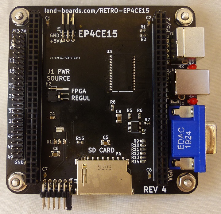
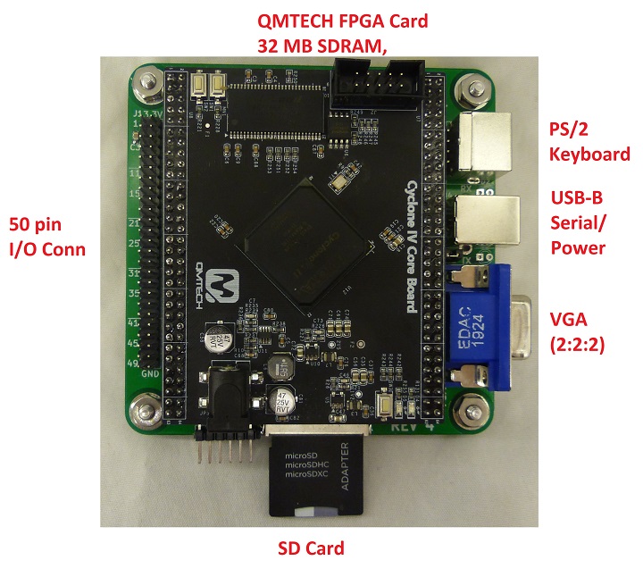
- RETRO-EP4CE15 FPGA base board
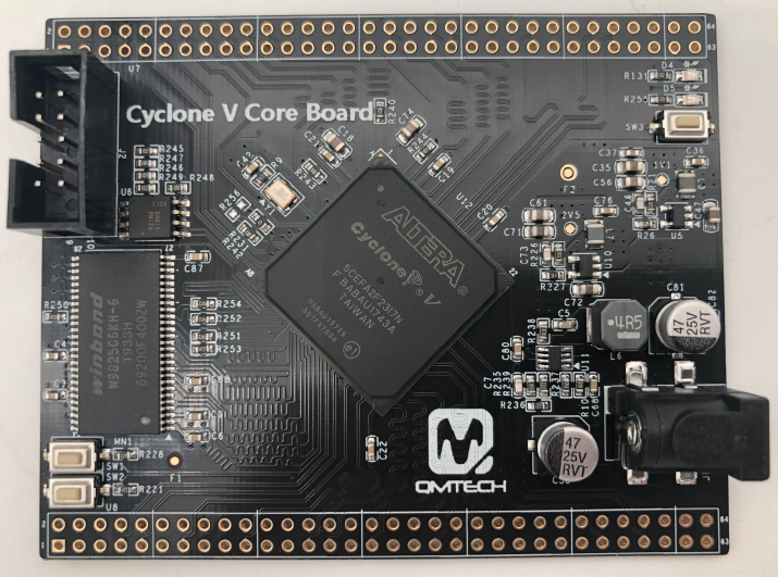
- FPGA card mounted on base board
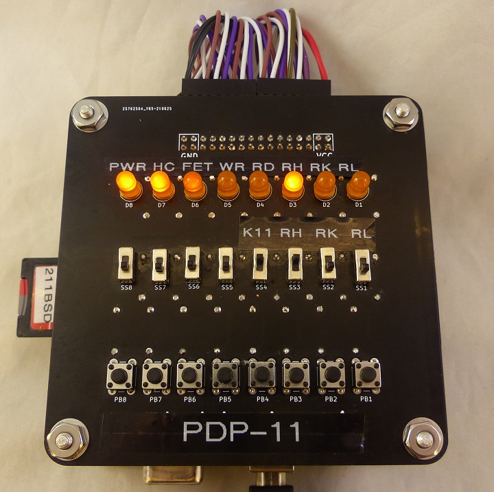
- LEDS-SWITCHES-2 board
Disks (SD card images) that work with PDP2011 build
PDP-11/45 Disks
DOS/BATCH-11 (rk05)
- DEC BATCH-11/DOS-11
- dos-batch - EC-11-ASDB-D PAL-11R Assembler Programmers Manual May71
- DOS/BATCH-11 (rk05) Disk Image
- Write to SD card - used Balena Etcher (windows) to write SD card
RT-11 4.0 (rk05)
- RT-11 4.0 (rk05) Disk Image
- Write to SD card - used Balena Etcher (windows) to write SD card
RT-11FB 4.0 (rk05)
- RT-11FB 4.0 (rk05)
RT-11 5.4 (rk05)
- RT-11 5.4 (rk05) Disk Image
- Write to SD card - used Balena Etcher (windows) to write SD card
UNIX V7 (rl02)
- UNIX V7 (rl02) Disk Image
- Write to SD card - used Balena Etcher (windows) to write SD card
PDP-11/70 disks
211BSD (rp06)
- 211BSD (rp06) Disk Image
- Write to SD card - used Balena Etcher (windows) to write SD card
RSX-11M PLUS 3.0 (rp06)
- RSX-11M PLUS 3.0 (rp06) Disk Image
- Write to SD card - used Balena Etcher (windows) to write SD card
Other Disk Images
- RL images are in chunks of 256 bytes, and require inserting 256 bytes padding after each of those chunks
- sdfmt converts files to 256 out of 512 bytes - Runs under Linux
- System Disk Images
- Disk Images
- W11 OS Disk sets - Well documented
- OS Kits
Other PDP2011 Builds
- PDP2011 by Sytse van Slooten - the original project
- David Richards PDP-11 Build on A-ESTF V2 EP4CE22 Board
- W11 PDP-11/70 Project
Software
Documentation
- PDP-11 Processor Handbook 1981 - on BitSavers
- PDP-11/45 System User's Manual
- PDP-11/70 Processor Handbook
PDP-11 Front Panel
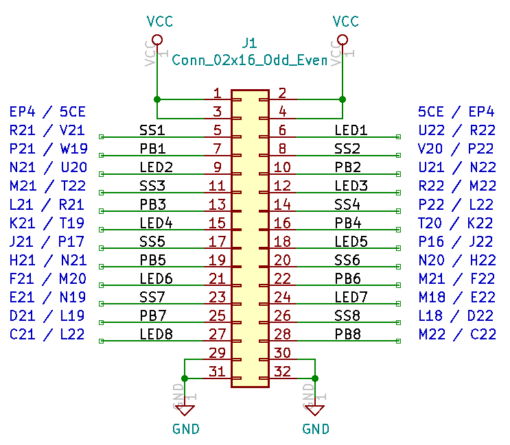
Front Panel Pins Directly Mapped to RETRO-EP4CE15
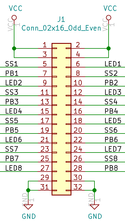
Front Panel J1
- Front Panel Card cables up to 50-pin connector on RETRO-EP4CE15 Card
- 32-pin connector
- Wiring "flipped" and directly in order
- Note extra ground/power pins on the Front Panel card
I/O Connector (5CEFA2F23 FPGA Card pin numbers)
| Function | Marking | 5CEFA2 FPGA Pin |
|---|---|---|
| resetbtn pushbutton | PB8 | PIN_M22 |
| PWR LED | D8 | PIN_L22 |
| sdHC LED | D7 | PIN_M18 |
| FETch LED | D6 | PIN_M20 |
| sdWR LED | D5 | PIN_P16 |
| sdRD LED | D4 | PIN_T19 |
| RH Drive (rp) LED | D3 | PIN_R22 |
| RK Drive LED | D2 | PIN_U20 |
| RL Drive LED | D1 | PIN_U22 |
| K11 (tty1) Slide switch | SS4 | PIN_P22 |
| RH Drive (rp) (UP) Slide switch | SS3 | PIN_T22 |
| RK Drive (UP) Slide switch | SS2 | PIN_V20 |
| RL Drive (UP) Slide switch | SS1 | PIN_V21 |
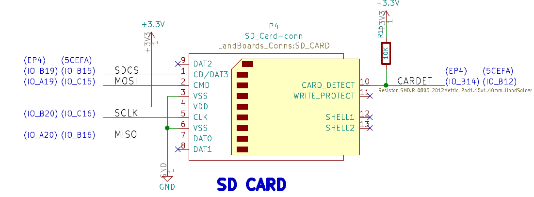
P4 - SD Card (5CEFA2F23 FPGA pin numbers)
- This build only works with SD Cards, not SD/HC or other newer cards.
- These cards are 1 GB or 2 GB in size.
- SDCS = U7-57 = PIN_B15
- MOSI = U7-58 = PIN_C15
- SCK = U7-59 = PIN_C16
- MISO = U7-60 = PIN_B16
- SD_DETECT - PIN_B12
MultiComp in Box Pins Mapping
Slide Switches/Reset Pushbutton
- Slide switches are on the bottom of the box
- PIN_L17 - Slide Switch 1 (top switch) - RL Drive select
- PIN_K17 - Slide Switch 2 - RK Drive select
- PIN_K22 - Slide Switch 3 - RH/RP Drive select
- PIN_K21 - Slide Switch 4 (bottom switch)
- Reset switch is on the front of the boz
- PIN_N16 - Reset Switch
SD Card
- External SD Card
- Install J3 on SD Card
- Runs card off 3.3V
- NO5V jumper installed
| J1 PIN | SIGNAL | COLOR | SD PIN | FPGA Pin | DIR |
|---|---|---|---|---|---|
| 2 | 3.3V | ORG | 7 | VREG 3.3V | OUT (PWR) |
| 45 | sdSCLK | GRY | 3 | PIN_L19 | OUT |
| 46 | sdMISO | BLU | 2 | PIN_L18 | IN |
| 47 | sdMOSI | WHT | 4 | PIN_L22 | OUT |
| 48 | sdCS | VIO | 5 | PIN_M22 | OUT |
| 49 | GND | GRN | 1 | GND | OUT (PWR) |
MultiComp DB-25 Pinout
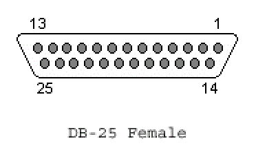
- MultiComp in a Box has a DB-25 Female connector
- DB25-02 - DB-25 adapter with Male connector
- Front panel card has 32-pin connector
- Dupont pin cable connects the two cards
- DB-25F on MultiComp in a Box as viewed from front of box
Front Panel Pinout
MultiComp in Box Front Panel Cabling
| DB25F | P1(DB25-02) | FPGA J1 | Signal | SW-J1 | FPGA | DB25F | P1(DB25-02) | FPGA J1 | Signal | SW-J1 | FPGA | |
|---|---|---|---|---|---|---|---|---|---|---|---|---|
| 1 | 25 | 26 | NC | |||||||||
| 2 | 23 | GND | 32 | 14 | 24 | GND | ||||||
| 3 | 21 | 44 | SS1 | 5 | PIN_M18 | 15 | 22 | 43 | SS2 | 8 | PIN_N19 | |
| 4 | 19 | 42 | SS3 | 11 | PIN_M21 | 16 | 20 | 41 | SS4 | 14 | PIN_M20 | |
| 5 | 17 | 40 | N/C | PIN_N20 | 17 | 18 | 39 | N/C | PIN_N21 | |||
| 6 | 15 | 38 | LED1 | 6 | PIN_P16 | 18 | 16 | 37 | LED2 | 9 | PIN_P17 | |
| 7 | 13 | 36 | LED3 | 12 | PIN_T20 | 19 | 14 | 35 | LED4 | 15 | PIN_T19 | |
| 8 | 11 | 34 | LED5 | 18 | PIN_P22 | 20 | 12 | 33 | LED6 | 21 | PIN_R21 | |
| 9 | 9 | 32 | LED7 | 24 | PIN_R22 | 21 | 10 | 31 | LED8 | 27 | PIN_T22 | |
| 10 | 7 | 30 | PB8 | 28 | PIN_U21 | 22 | 8 | 29 | PIN_U20 | |||
| 11 | 5 | 23 | 6 | |||||||||
| 12 | 3 | 24 | 4 | |||||||||
| 13 | 1 | +3.3V | 2 | 25 | 2 | +3.3V |
Connectors on RETROEP4-CE15 Card
P1 - VGA
- videoR0 = U8-49 = PIN_E12
- videoR1 = U8-50 = PIN_D12
- videoG0 = U8-51 = PIN_D13
- videoG1 = U8-52 = PIN_C13
- videoB0 = U8-53 = PIN_B13
- videoB1 = U8-54 = PIN_A13
- hSync = U8-55 = PIN_A15
- vSync = U8-56 = PIN_A14
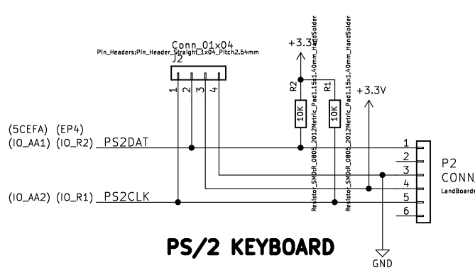
P2 - PS/2 Keyboard
- PS2DAT = U7-8 = PIN_BANK_2A_AA1
- PS2CLK = U7-8 = PIN_NANK_2A_AA2
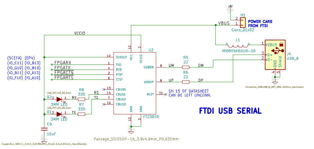
P3 - Serial Ports - I/O connector
- fpgaRx1 (in) = PIN_C11
- Needs weak pullup
- set_instance_assignment -name WEAK_PULL_UP_RESISTOR ON -to rxd1
- Needs weak pullup
- fpgaTx1 (out) = PIN_G10
- fpgaRts1 = U7-44 = PIN_F10
- fpgaCts1 = U7-46 = PIN_B11
IO conn
- Second serial port on I/O connector
- rx2 (in) = PIN_M18
- tx2 (out) = PIN_L19
- rts2 (out) = PIN_N19
- cts2 (in) = PIN_M21
J4 - USB-B B (5CEFA2F23 FPGA Card pin numbers) Serial Port
- On-board FT230X FTDI USB to Serial
FPGA Resources
- PDP-11/70
- Front Panel
- In MultiComp Box
+-------------------------------------------------------------------------------+
; Fitter Summary                                                                ;
+---------------------------------+---------------------------------------------+
; Fitter Status                   ; Successful - Sat Apr 30 19:30:51 2022       ;
; Quartus Prime Version           ; 21.1.0 Build 842 10/21/2021 SJ Lite Edition ;
; Revision Name                   ; top                                         ;
; Top-level Entity Name           ; top                                         ;
; Family                          ; Cyclone V                                   ;
; Device                          ; 5CEFA2F23I7                                 ;
; Timing Models                   ; Final                                       ;
; Logic utilization (in ALMs)     ; 7,809 / 9,430 ( 83 % )                      ;
; Total registers                 ; 6016                                        ;
; Total pins                      ; 76 / 224 ( 34 % )                           ;
; Total virtual pins              ; 0                                           ;
; Total block memory bits         ; 180,224 / 1,802,240 ( 10 % )                ;
; Total RAM Blocks                ; 25 / 176 ( 14 % )                           ;
; Total DSP Blocks                ; 1 / 25 ( 4 % )                              ;
; Total HSSI RX PCSs              ; 0                                           ;
; Total HSSI PMA RX Deserializers ; 0                                           ;
; Total HSSI TX PCSs              ; 0                                           ;
; Total HSSI PMA TX Serializers   ; 0                                           ;
; Total PLLs                      ; 1 / 4 ( 25 % )                              ;
; Total DLLs                      ; 0 / 4 ( 0 % )                               ;
+---------------------------------+---------------------------------------------+
External Resources
- PDP2011 by Sytse van Slooten
- Active as of 2021-11
- David J Richards PDP-11 Build - copied and adapted from pdp2011 by Sytse van Slooten
- PDP-11 on BitSavers
- Scott L Baker PDP11-SOC
- PDP-11/20 CPU
- UART + Timer + I/O Ports coded in VHDL
- 8KB RAM
- Implemented on the Lattice iCE40-hx8k dev board
- w11: PDP 11/70 CPU and SoC
- PDP-11/70 CPU with memory management unit, but without floating point unit,
- Quick start Guide
- OS Kits (Disk Images)
- Guide to run operating system images on w11a systems
- Guide to install and build w11a systems, test benches and support software
Programming the FPGA EEPROM (5CEFA2F23 FPGA)
- File
- Convert Programming File
- Configuration Device = MT25QL128
- Mode = Active Serial
- Programming File Type: *.jic
- Advanced = Check both Disables...
- Select Flash Loader
- Add Device = Cyclone V and 5CEFA2
- Select SOF Data
- Select Add File and select the .sof file
- Generate
- In Tools, Programmer
- Mode: JTAG
- Add file and select the .jic file
- Select Program/Configure
- Takes a while to program
- Press button near VGA
Pin Lists
Pin List Standalone with Front Panel
- With LEDS-SWITCHES-2 card
| To | Direction | Location | I/O Standard | Pull-Up |
|---|---|---|---|---|
| clkin | Input | PIN_M9 | 3.3-V LVTTL | |
| cts1 | Input | PIN_B11 | 3.3-V LVTTL | |
| dram_addr[0] | Output | PIN_P8 | 3.3-V LVTTL | |
| dram_addr[1] | Output | PIN_P7 | 3.3-V LVTTL | |
| dram_addr[10] | Output | PIN_R6 | 3.3-V LVTTL | |
| dram_addr[11] | Output | PIN_T9 | 3.3-V LVTTL | |
| dram_addr[12] | Output | PIN_Y9 | 3.3-V LVTTL | |
| dram_addr[2] | Output | PIN_N8 | 3.3-V LVTTL | |
| dram_addr[3] | Output | PIN_N6 | 3.3-V LVTTL | |
| dram_addr[4] | Output | PIN_U6 | 3.3-V LVTTL | |
| dram_addr[5] | Output | PIN_U7 | 3.3-V LVTTL | |
| dram_addr[6] | Output | PIN_V6 | 3.3-V LVTTL | |
| dram_addr[7] | Output | PIN_U8 | 3.3-V LVTTL | |
| dram_addr[8] | Output | PIN_T8 | 3.3-V LVTTL | |
| dram_addr[9] | Output | PIN_W8 | 3.3-V LVTTL | |
| dram_ba_0 | Output | PIN_T7 | 3.3-V LVTTL | |
| dram_ba_1 | Output | PIN_P9 | 3.3-V LVTTL | |
| dram_cas_n | Output | PIN_AA7 | 3.3-V LVTTL | |
| dram_cke | Output | PIN_V9 | 3.3-V LVTTL | |
| dram_clk | Output | PIN_AB11 | 3.3-V LVTTL | |
| dram_cs_n | Output | PIN_AB5 | 3.3-V LVTTL | |
| dram_dq[0] | Bidir | PIN_AA12 | 3.3-V LVTTL | |
| dram_dq[1] | Bidir | PIN_Y11 | 3.3-V LVTTL | |
| dram_dq[10] | Bidir | PIN_U11 | 3.3-V LVTTL | |
| dram_dq[11] | Bidir | PIN_R10 | 3.3-V LVTTL | |
| dram_dq[12] | Bidir | PIN_R11 | 3.3-V LVTTL | |
| dram_dq[13] | Bidir | PIN_U12 | 3.3-V LVTTL | |
| dram_dq[14] | Bidir | PIN_R12 | 3.3-V LVTTL | |
| dram_dq[15] | Bidir | PIN_P12 | 3.3-V LVTTL | |
| dram_dq[2] | Bidir | PIN_AA10 | 3.3-V LVTTL | |
| dram_dq[3] | Bidir | PIN_AB10 | 3.3-V LVTTL | |
| dram_dq[4] | Bidir | PIN_Y10 | 3.3-V LVTTL | |
| dram_dq[5] | Bidir | PIN_AA9 | 3.3-V LVTTL | |
| dram_dq[6] | Bidir | PIN_AB8 | 3.3-V LVTTL | |
| dram_dq[7] | Bidir | PIN_AA8 | 3.3-V LVTTL | |
| dram_dq[8] | Bidir | PIN_U10 | 3.3-V LVTTL | |
| dram_dq[9] | Bidir | PIN_T10 | 3.3-V LVTTL | |
| dram_ldqm | Output | PIN_AB7 | 3.3-V LVTTL | |
| dram_ras_n | Output | PIN_AB6 | 3.3-V LVTTL | |
| dram_udqm | Output | PIN_V10 | 3.3-V LVTTL | |
| dram_we_n | Output | PIN_W9 | 3.3-V LVTTL | |
| i_PB[1] | Input | PIN_W19 | 3.3-V LVTTL | |
| i_PB[2] | Input | PIN_U21 | 3.3-V LVTTL | |
| i_PB[3] | Input | PIN_R21 | 3.3-V LVTTL | |
| i_PB[4] | Input | PIN_T20 | 3.3-V LVTTL | |
| i_PB[5] | Input | PIN_N21 | 3.3-V LVTTL | |
| i_PB[6] | Input | PIN_M21 | 3.3-V LVTTL | |
| i_PB[7] | Input | PIN_L19 | 3.3-V LVTTL | |
| i_PB[8] | Input | PIN_M22 | 3.3-V LVTTL | |
| i_SS[1] | Input | PIN_V21 | 3.3-V LVTTL | |
| i_SS[2] | Input | PIN_V20 | 3.3-V LVTTL | |
| i_SS[3] | Input | PIN_T22 | 3.3-V LVTTL | |
| i_SS[4] | Input | PIN_P22 | 3.3-V LVTTL | |
| i_SS[5] | Input | PIN_P17 | 3.3-V LVTTL | |
| i_SS[6] | Input | PIN_N20 | 3.3-V LVTTL | |
| i_SS[7] | Input | PIN_N19 | 3.3-V LVTTL | |
| i_SS[8] | Input | PIN_L18 | 3.3-V LVTTL | |
| o_LED[1] | Output | PIN_U22 | 3.3-V LVTTL | |
| o_LED[2] | Output | PIN_U20 | 3.3-V LVTTL | |
| o_LED[3] | Output | PIN_R22 | 3.3-V LVTTL | |
| o_LED[4] | Output | PIN_T19 | 3.3-V LVTTL | |
| o_LED[5] | Output | PIN_P16 | 3.3-V LVTTL | |
| o_LED[6] | Output | PIN_M20 | 3.3-V LVTTL | |
| o_LED[7] | Output | PIN_M18 | 3.3-V LVTTL | |
| o_LED[8] | Output | PIN_L22 | 3.3-V LVTTL | |
| ps2k_c | Input | PIN_AA2 | 3.3-V LVTTL | |
| ps2k_d | Input | PIN_AA1 | 3.3-V LVTTL | |
| rts1 | Output | PIN_F10 | 3.3-V LVTTL | |
| rx1 | Input | PIN_C11 | 3.3-V LVTTL | |
| sdcard_cs | Output | PIN_B15 | 3.3-V LVTTL | |
| sdcard_miso | Input | PIN_B16 | 3.3-V LVTTL | |
| sdcard_mosi | Output | PIN_C15 | 3.3-V LVTTL | |
| sdcard_sclk | Output | PIN_C16 | 3.3-V LVTTL | |
| tx1 | Output | PIN_G10 | 3.3-V LVTTL | |
| vgab[0] | Output | PIN_B13 | 3.3-V LVTTL | |
| vgab[1] | Output | PIN_A13 | 3.3-V LVTTL | |
| vgag[0] | Output | PIN_D13 | 3.3-V LVTTL | |
| vgag[1] | Output | PIN_C13 | 3.3-V LVTTL | |
| vgah | Output | PIN_A15 | 3.3-V LVTTL | |
| vgar[0] | Output | PIN_E12 | 3.3-V LVTTL | |
| vgar[1] | Output | PIN_D12 | 3.3-V LVTTL | |
| vgav | Output | PIN_A14 | 3.3-V LVTTL | |
| xu_cs | Output | 3.3-V LVTTL | ||
| xu_debug_tx | Output | 3.3-V LVTTL | ||
| xu_miso | Input | 3.3-V LVTTL | ||
| xu_mosi | Output | 3.3-V LVTTL | ||
| xu_sclk | Output | 3.3-V LVTTL |
qsf Standalone file with Front Panel
set_global_assignment -name FAMILY "Cyclone V"
set_global_assignment -name DEVICE 5CEFA2F23I7
set_global_assignment -name TOP_LEVEL_ENTITY top
set_global_assignment -name ORIGINAL_QUARTUS_VERSION 9.0
set_global_assignment -name PROJECT_CREATION_TIME_DATE "23:14:32  MARCH 19, 2009"
set_global_assignment -name LAST_QUARTUS_VERSION "21.1.0 Lite Edition"
set_global_assignment -name STRATIX_DEVICE_IO_STANDARD "3.3-V LVTTL"
set_global_assignment -name CYCLONEII_RESERVE_NCEO_AFTER_CONFIGURATION "USE AS REGULAR IO"
set_global_assignment -name RESERVE_ASDO_AFTER_CONFIGURATION "AS INPUT TRI-STATED"
set_global_assignment -name MIN_CORE_JUNCTION_TEMP "-40"
set_global_assignment -name MAX_CORE_JUNCTION_TEMP 100
set_global_assignment -name POWER_PRESET_COOLING_SOLUTION "23 MM HEAT SINK WITH 200 LFPM AIRFLOW"
set_global_assignment -name POWER_BOARD_THERMAL_MODEL "NONE (CONSERVATIVE)"
# Clock
set_location_assignment PIN_M9 -to clkin
# Pushbuttons on LEDS-SWITCHES-2 card
set_location_assignment PIN_M22 -to i_PB[8]
set_location_assignment PIN_L19 -to i_PB[7]
set_location_assignment PIN_M21 -to i_PB[6]
set_location_assignment PIN_N21 -to i_PB[5]
set_location_assignment PIN_T20 -to i_PB[4]
set_location_assignment PIN_R21 -to i_PB[3]
set_location_assignment PIN_U21 -to i_PB[2]
set_location_assignment PIN_W19 -to i_PB[1]
set_location_assignment PIN_L18 -to i_SS[8]
set_location_assignment PIN_N19 -to i_SS[7]
set_location_assignment PIN_N20 -to i_SS[6]
set_location_assignment PIN_P17 -to i_SS[5]
set_location_assignment PIN_P22 -to i_SS[4]
set_location_assignment PIN_T22 -to i_SS[3]
set_location_assignment PIN_V20 -to i_SS[2]
set_location_assignment PIN_V21 -to i_SS[1]
# LEDs on LEDS-SWITCHES-2 card
set_location_assignment PIN_L22 -to o_LED[8]
set_location_assignment PIN_M18 -to o_LED[7]
set_location_assignment PIN_M20 -to o_LED[6]
set_location_assignment PIN_P16 -to o_LED[5]
set_location_assignment PIN_T19 -to o_LED[4]
set_location_assignment PIN_R22 -to o_LED[3]
set_location_assignment PIN_U20 -to o_LED[2]
set_location_assignment PIN_U22 -to o_LED[1]
# SDRAM
set_location_assignment PIN_Y9 -to dram_addr[12]
set_location_assignment PIN_T9 -to dram_addr[11]
set_location_assignment PIN_R6 -to dram_addr[10]
set_location_assignment PIN_W8 -to dram_addr[9]
set_location_assignment PIN_T8 -to dram_addr[8]
set_location_assignment PIN_U8 -to dram_addr[7]
set_location_assignment PIN_V6 -to dram_addr[6]
set_location_assignment PIN_U7 -to dram_addr[5]
set_location_assignment PIN_U6 -to dram_addr[4]
set_location_assignment PIN_N6 -to dram_addr[3]
set_location_assignment PIN_N8 -to dram_addr[2]
set_location_assignment PIN_P7 -to dram_addr[1]
set_location_assignment PIN_P8 -to dram_addr[0]
set_location_assignment PIN_P9 -to dram_ba_1
set_location_assignment PIN_T7 -to dram_ba_0
set_location_assignment PIN_AA7 -to dram_cas_n
set_location_assignment PIN_V9 -to dram_cke
set_location_assignment PIN_AB11 -to dram_clk
set_location_assignment PIN_AB5 -to dram_cs_n
set_location_assignment PIN_P12 -to dram_dq[15]
set_location_assignment PIN_R12 -to dram_dq[14]
set_location_assignment PIN_U12 -to dram_dq[13]
set_location_assignment PIN_R11 -to dram_dq[12]
set_location_assignment PIN_R10 -to dram_dq[11]
set_location_assignment PIN_U11 -to dram_dq[10]
set_location_assignment PIN_T10 -to dram_dq[9]
set_location_assignment PIN_U10 -to dram_dq[8]
set_location_assignment PIN_AA8 -to dram_dq[7]
set_location_assignment PIN_AB8 -to dram_dq[6]
set_location_assignment PIN_AA9 -to dram_dq[5]
set_location_assignment PIN_Y10 -to dram_dq[4]
set_location_assignment PIN_AB10 -to dram_dq[3]
set_location_assignment PIN_AA10 -to dram_dq[2]
set_location_assignment PIN_Y11 -to dram_dq[1]
set_location_assignment PIN_AA12 -to dram_dq[0]
set_location_assignment PIN_V10 -to dram_udqm
set_location_assignment PIN_AB7 -to dram_ldqm
set_location_assignment PIN_AB6 -to dram_ras_n
set_location_assignment PIN_W9 -to dram_we_n
# Serial port (USB-to-Serial)
set_location_assignment PIN_C11 -to rx1
set_location_assignment PIN_G10 -to tx1
set_location_assignment PIN_F10 -to rts1
set_location_assignment PIN_B11 -to cts1
# Second serial port
# SD Card
set_location_assignment PIN_C16 -to sdcard_sclk
set_location_assignment PIN_B15 -to sdcard_cs
set_location_assignment PIN_B16 -to sdcard_miso
set_location_assignment PIN_C15 -to sdcard_mosi
# Ethernet
# PS/2 Keyboard
set_location_assignment PIN_AA2 -to ps2k_c
set_location_assignment PIN_AA1 -to ps2k_d
# Video
set_location_assignment PIN_E12 -to vgar[0]
set_location_assignment PIN_D12 -to vgar[1]
set_location_assignment PIN_B13 -to vgab[0]
set_location_assignment PIN_A13 -to vgab[1]
set_location_assignment PIN_D13 -to vgag[0]
set_location_assignment PIN_C13 -to vgag[1]
set_location_assignment PIN_A15 -to vgah
set_location_assignment PIN_A14 -to vgav
Pin List Standalone
qsf file Standalone
set_global_assignment -name FAMILY "Cyclone V"
set_global_assignment -name DEVICE 5CEFA2F23I7
set_global_assignment -name TOP_LEVEL_ENTITY top
set_global_assignment -name ORIGINAL_QUARTUS_VERSION 9.0
set_global_assignment -name PROJECT_CREATION_TIME_DATE "23:14:32  MARCH 19, 2009"
set_global_assignment -name LAST_QUARTUS_VERSION "21.1.0 Lite Edition"
set_global_assignment -name STRATIX_DEVICE_IO_STANDARD "3.3-V LVTTL"
set_global_assignment -name CYCLONEII_RESERVE_NCEO_AFTER_CONFIGURATION "USE AS REGULAR IO"
set_global_assignment -name RESERVE_ASDO_AFTER_CONFIGURATION "AS INPUT TRI-STATED"
set_location_assignment PIN_M9 -to clkin
set_location_assignment PIN_M22 -to resetbtn
set_instance_assignment -name WEAK_PULL_UP_RESISTOR ON -to resetbtn
# Control switches
# Jumpers on front edge
# SDRAM
set_location_assignment PIN_Y9 -to dram_addr[12]
set_location_assignment PIN_T9 -to dram_addr[11]
set_location_assignment PIN_R6 -to dram_addr[10]
set_location_assignment PIN_W8 -to dram_addr[9]
set_location_assignment PIN_T8 -to dram_addr[8]
set_location_assignment PIN_U8 -to dram_addr[7]
set_location_assignment PIN_V6 -to dram_addr[6]
set_location_assignment PIN_U7 -to dram_addr[5]
set_location_assignment PIN_U6 -to dram_addr[4]
set_location_assignment PIN_N6 -to dram_addr[3]
set_location_assignment PIN_N8 -to dram_addr[2]
set_location_assignment PIN_P7 -to dram_addr[1]
set_location_assignment PIN_P8 -to dram_addr[0]
set_location_assignment PIN_P9 -to dram_ba_1
set_location_assignment PIN_T7 -to dram_ba_0
set_location_assignment PIN_AA7 -to dram_cas_n
set_location_assignment PIN_V9 -to dram_cke
set_location_assignment PIN_AB11 -to dram_clk
set_location_assignment PIN_AB5 -to dram_cs_n
set_location_assignment PIN_P12 -to dram_dq[15]
set_location_assignment PIN_R12 -to dram_dq[14]
set_location_assignment PIN_U12 -to dram_dq[13]
set_location_assignment PIN_R11 -to dram_dq[12]
set_location_assignment PIN_R10 -to dram_dq[11]
set_location_assignment PIN_U11 -to dram_dq[10]
set_location_assignment PIN_T10 -to dram_dq[9]
set_location_assignment PIN_U10 -to dram_dq[8]
set_location_assignment PIN_AA8 -to dram_dq[7]
set_location_assignment PIN_AB8 -to dram_dq[6]
set_location_assignment PIN_AA9 -to dram_dq[5]
set_location_assignment PIN_Y10 -to dram_dq[4]
set_location_assignment PIN_AB10 -to dram_dq[3]
set_location_assignment PIN_AA10 -to dram_dq[2]
set_location_assignment PIN_Y11 -to dram_dq[1]
set_location_assignment PIN_AA12 -to dram_dq[0]
set_location_assignment PIN_V10 -to dram_udqm
set_location_assignment PIN_AB7 -to dram_ldqm
set_location_assignment PIN_AB6 -to dram_ras_n
set_location_assignment PIN_W9 -to dram_we_n
# Serial port (USB-to-Serial)
set_location_assignment PIN_L19 -to rx1
set_location_assignment PIN_L18 -to tx1
set_location_assignment PIN_M18 -to rts1
set_location_assignment PIN_N19 -to cts1
# Second serial port
# SD Card
set_location_assignment PIN_C16 -to sdcard_sclk
set_location_assignment PIN_B15 -to sdcard_cs
set_location_assignment PIN_B16 -to sdcard_miso
set_location_assignment PIN_C15 -to sdcard_mosi
# Seven segment display (on J1)
# Ethernet
set_location_assignment PIN_T20 -to xu_cs
set_location_assignment PIN_P17 -to xu_debug_tx
set_location_assignment PIN_P16 -to xu_miso
set_location_assignment PIN_N21 -to xu_mosi
set_location_assignment PIN_N20 -to xu_sclk
# PS/2 Keyboard
set_location_assignment PIN_AA2 -to ps2k_c
set_location_assignment PIN_AA1 -to ps2k_d
# Video
set_location_assignment PIN_A15 -to vgah
set_location_assignment PIN_A14 -to vgav

set_global_assignment -name PARTITION_NETLIST_TYPE SOURCE -section_id Top
set_global_assignment -name PARTITION_FITTER_PRESERVATION_LEVEL PLACEMENT_AND_ROUTING -section_id Top
set_global_assignment -name PARTITION_COLOR 16764057 -section_id Top

set_global_assignment -name MIN_CORE_JUNCTION_TEMP "-40"
set_global_assignment -name MAX_CORE_JUNCTION_TEMP 100
set_global_assignment -name POWER_PRESET_COOLING_SOLUTION "23 MM HEAT SINK WITH 200 LFPM AIRFLOW"
set_global_assignment -name POWER_BOARD_THERMAL_MODEL "NONE (CONSERVATIVE)"
set_location_assignment PIN_E12 -to vgar[0]
set_location_assignment PIN_D12 -to vgar[1]
set_location_assignment PIN_B13 -to vgab[0]
set_location_assignment PIN_A13 -to vgab[1]
set_location_assignment PIN_D13 -to vgag[0]
set_location_assignment PIN_C13 -to vgag[1]
set_location_assignment PIN_L17 -to sw[0]
set_location_assignment PIN_K17 -to sw[1]
set_location_assignment PIN_K22 -to sw[2]
set_location_assignment PIN_K21 -to sw[3]
set_location_assignment PIN_M16 -to sw[4]
set_location_assignment PIN_N16 -to sw[5]
set_location_assignment PIN_R21 -to greenled[0]
set_location_assignment PIN_P22 -to greenled[1]
set_location_assignment PIN_T22 -to greenled[2]
set_location_assignment PIN_R22 -to greenled[3]
set_location_assignment PIN_U20 -to greenled[4]
set_global_assignment -name VHDL_FILE ../vgacr.vhd
set_global_assignment -name VHDL_FILE ../vga.vhd
set_global_assignment -name VHDL_FILE ../vt.vhd
set_global_assignment -name VHDL_FILE ../ps2.vhd
set_global_assignment -name VHDL_FILE ../vgafont.vhd
set_global_assignment -name VHDL_FILE ../vtbrt42.vhd
set_global_assignment -name VHDL_FILE ../sdspi.vhd
set_global_assignment -name VHDL_FILE ../mnckw.vhd
set_global_assignment -name VHDL_FILE ../mncdo.vhd
set_global_assignment -name VHDL_FILE ../mncdi.vhd
set_global_assignment -name VHDL_FILE ../mncad.vhd
set_global_assignment -name VHDL_FILE ../mncaa.vhd
set_global_assignment -name VHDL_FILE ../m9312h47.vhd
set_global_assignment -name VHDL_FILE ../m9312l47.vhd
set_global_assignment -name VHDL_FILE ../dr11c.vhd
set_global_assignment -name VHDL_FILE ../panelos.vhd
set_global_assignment -name VHDL_FILE ../paneldriver.vhd
set_global_assignment -name VHDL_FILE ../paneldb.vhd
set_global_assignment -name VHDL_FILE ../xubrt45.vhd
set_global_assignment -name VHDL_FILE ../xubm.vhd
set_global_assignment -name VHDL_FILE ../xubl.vhd
set_global_assignment -name VHDL_FILE ../xu.vhd
set_global_assignment -name VHDL_FILE ../rh11.vhd
set_global_assignment -name VHDL_FILE ../kl11.vhd
set_global_assignment -name VHDL_FILE ../rk11.vhd
set_global_assignment -name VHDL_FILE ../unibus.vhd
set_global_assignment -name VHDL_FILE ../cr.vhd
set_global_assignment -name VHDL_FILE ../rl11.vhd
set_global_assignment -name VHDL_FILE ../mmu.vhd
set_global_assignment -name VHDL_FILE ../kw11l.vhd
set_global_assignment -name VHDL_FILE ../fpuregs.vhd
set_global_assignment -name VHDL_FILE ../csdr.vhd
set_global_assignment -name VHDL_FILE ../cpuregs.vhd
set_global_assignment -name VHDL_FILE ../cpu.vhd
set_global_assignment -name VHDL_FILE top.vhd
set_global_assignment -name VHDL_FILE ssegdecoder.vhd
set_global_assignment -name CDF_FILE top.cdf
set_global_assignment -name QIP_FILE pll.qip
set_instance_assignment -name PARTITION_HIERARCHY root_partition -to | -section_id Top
Pin List in MultiComp Box
| To | Direction | Location | Pull-Up |
|---|---|---|---|
| clkin | Input | PIN_M9 | |
| cts1 | Input | PIN_B11 | on |
| dram_addr[12] | Output | PIN_Y9 | |
| dram_addr[11] | Output | PIN_T9 | |
| dram_addr[10] | Output | PIN_R6 | |
| dram_addr[9] | Output | PIN_W8 | |
| dram_addr[8] | Output | PIN_T8 | |
| dram_addr[7] | Output | PIN_U8 | |
| dram_addr[6] | Output | PIN_V6 | |
| dram_addr[5] | Output | PIN_U7 | |
| dram_addr[4] | Output | PIN_U6 | |
| dram_addr[3] | Output | PIN_N6 | |
| dram_addr[2] | Output | PIN_N8 | |
| dram_addr[1] | Output | PIN_P7 | |
| dram_addr[0] | Output | PIN_P8 | |
| dram_ba_0 | Output | PIN_T7 | |
| dram_ba_1 | Output | PIN_P9 | |
| dram_cas_n | Output | PIN_AA7 | |
| dram_cke | Output | PIN_V9 | |
| dram_clk | Output | PIN_AB11 | |
| dram_cs_n | Output | PIN_AB5 | |
| dram_dq[15] | Bidir | PIN_P12 | |
| dram_dq[14] | Bidir | PIN_R12 | |
| dram_dq[13] | Bidir | PIN_U12 | |
| dram_dq[12] | Bidir | PIN_R11 | |
| dram_dq[11] | Bidir | PIN_R10 | |
| dram_dq[10] | Bidir | PIN_U11 | |
| dram_dq[9] | Bidir | PIN_T10 | |
| dram_dq[8] | Bidir | PIN_U10 | |
| dram_dq[7] | Bidir | PIN_AA8 | |
| dram_dq[6] | Bidir | PIN_AB8 | |
| dram_dq[5] | Bidir | PIN_AA9 | |
| dram_dq[4] | Bidir | PIN_Y10 | |
| dram_dq[3] | Bidir | PIN_AB10 | |
| dram_dq[2] | Bidir | PIN_AA10 | |
| dram_dq[1] | Bidir | PIN_Y11 | |
| dram_dq[0] | Bidir | PIN_AA12 | |
| dram_ldqm | Output | PIN_AB7 | |
| dram_ras_n | Output | PIN_AB6 | |
| dram_udqm | Output | PIN_V10 | |
| dram_we_n | Output | PIN_W9 | |
| i_PB[8] | Input | PIN_N16 | on |
| i_PB[7] | Input | PIN_Y20 | on |
| i_PB[6] | Input | PIN_M21 | on |
| i_PB[5] | Input | PIN_N21 | on |
| i_PB[4] | Input | PIN_T20 | on |
| i_PB[3] | Input | PIN_R21 | on |
| i_PB[2] | Input | PIN_U21 | on |
| i_PB[1] | Input | PIN_W19 | on |
| i_SS[8] | Input | PIN_P22 | on |
| i_SS[7] | Input | PIN_N19 | on |
| i_SS[6] | Input | PIN_N20 | on |
| i_SS[5] | Input | PIN_M16 | on |
| i_SS[4] | Input | PIN_K21 | on |
| i_SS[3] | Input | PIN_K22 | on |
| i_SS[2] | Input | PIN_K17 | on |
| i_SS[1] | Input | PIN_L17 | on |
| o_LED[8] | Output | PIN_P17 | |
| o_LED[7] | Output | PIN_M18 | |
| o_LED[6] | Output | PIN_M20 | |
| o_LED[5] | Output | PIN_P16 | |
| o_LED[4] | Output | PIN_T19 | |
| o_LED[3] | Output | PIN_R22 | |
| o_LED[2] | Output | PIN_U20 | |
| o_LED[1] | Output | PIN_U22 | |
| ps2k_c | Input | PIN_AA2 | on |
| ps2k_d | Input | PIN_AA1 | on |
| rts1 | Output | PIN_F10 | |
| rx1 | Input | PIN_C11 | on |
| sdcard_cs | Output | PIN_M22 | |
| sdcard_miso | Input | PIN_L18 | on |
| sdcard_mosi | Output | PIN_L22 | |
| sdcard_sclk | Output | PIN_L19 | |
| tx1 | Output | PIN_G10 | |
| vgab[1] | Output | PIN_A13 | |
| vgab[0] | Output | PIN_B13 | |
| vgag[1] | Output | PIN_C13 | |
| vgag[0] | Output | PIN_D13 | |
| vgah | Output | PIN_A15 | |
| vgar[1] | Output | PIN_D12 | |
| vgar[0] | Output | PIN_E12 | |
| vgav | Output | PIN_A14 | |
| xu_cs | Output | PIN_AB22 | |
| xu_debug_tx | Output | PIN_AA22 | |
| xu_miso | Input | PIN_Y22 | on |
| xu_mosi | Output | PIN_V20 | |
| xu_sclk | Output | PIN_T22 |
qsf file in MultiComp Box
set_global_assignment -name FAMILY "Cyclone V"
set_global_assignment -name DEVICE 5CEFA2F23I7
set_global_assignment -name TOP_LEVEL_ENTITY top
set_global_assignment -name ORIGINAL_QUARTUS_VERSION 9.0
set_global_assignment -name PROJECT_CREATION_TIME_DATE "23:14:32  MARCH 19, 2009"
set_global_assignment -name LAST_QUARTUS_VERSION "21.1.0 Lite Edition"
set_global_assignment -name STRATIX_DEVICE_IO_STANDARD "3.3-V LVTTL"
set_global_assignment -name CYCLONEII_RESERVE_NCEO_AFTER_CONFIGURATION "USE AS REGULAR IO"
set_global_assignment -name RESERVE_ASDO_AFTER_CONFIGURATION "AS INPUT TRI-STATED"
set_global_assignment -name PARTITION_NETLIST_TYPE SOURCE -section_id Top
set_global_assignment -name PARTITION_FITTER_PRESERVATION_LEVEL PLACEMENT_AND_ROUTING -section_id Top
set_global_assignment -name PARTITION_COLOR 16764057 -section_id Top
set_global_assignment -name MIN_CORE_JUNCTION_TEMP "-40"
set_global_assignment -name MAX_CORE_JUNCTION_TEMP 100
set_global_assignment -name POWER_PRESET_COOLING_SOLUTION "23 MM HEAT SINK WITH 200 LFPM AIRFLOW"
set_global_assignment -name POWER_BOARD_THERMAL_MODEL "NONE (CONSERVATIVE)"
# Clock
set_location_assignment PIN_M9 -to clkin
# Serial port (USB-to-Serial)
set_location_assignment PIN_C11 -to rx1
set_location_assignment PIN_G10 -to tx1
set_location_assignment PIN_F10 -to rts1
set_location_assignment PIN_B11 -to cts1
set_instance_assignment -name WEAK_PULL_UP_RESISTOR ON -to cts1
set_instance_assignment -name WEAK_PULL_UP_RESISTOR ON -to rx1
# Second serial port
# SD Card
set_location_assignment PIN_L19 -to sdcard_sclk
set_location_assignment PIN_M22 -to sdcard_cs
set_location_assignment PIN_L18 -to sdcard_miso
set_instance_assignment -name WEAK_PULL_UP_RESISTOR ON -to sdcard_miso
set_location_assignment PIN_L22 -to sdcard_mosi
# PS/2 Keyboard
set_location_assignment PIN_AA2 -to ps2k_c
set_location_assignment PIN_AA1 -to ps2k_d
set_instance_assignment -name WEAK_PULL_UP_RESISTOR ON -to ps2k_c
set_instance_assignment -name WEAK_PULL_UP_RESISTOR ON -to ps2k_d
# Video
set_location_assignment PIN_A15 -to vgah
set_location_assignment PIN_A14 -to vgav
set_location_assignment PIN_E12 -to vgar[0]
set_location_assignment PIN_D12 -to vgar[1]
set_location_assignment PIN_B13 -to vgab[0]
set_location_assignment PIN_A13 -to vgab[1]
set_location_assignment PIN_D13 -to vgag[0]
set_location_assignment PIN_C13 -to vgag[1]
# LEDs
set_location_assignment PIN_U22 -to o_LED[1]
set_location_assignment PIN_R22 -to o_LED[3]
set_location_assignment PIN_U20 -to o_LED[2]
set_location_assignment PIN_P17 -to o_LED[8]
set_location_assignment PIN_M18 -to o_LED[7]
set_location_assignment PIN_M20 -to o_LED[6]
set_location_assignment PIN_P16 -to o_LED[5]
set_location_assignment PIN_T19 -to o_LED[4]
# Slide Switches
set_location_assignment PIN_L17 -to i_SS[1]
set_location_assignment PIN_K17 -to i_SS[2]
set_location_assignment PIN_K22 -to i_SS[3]
set_location_assignment PIN_K21 -to i_SS[4]
set_location_assignment PIN_M16 -to i_SS[5]
set_location_assignment PIN_N20 -to i_SS[6]
set_location_assignment PIN_N19 -to i_SS[7]
set_location_assignment PIN_P22 -to i_SS[8]
set_instance_assignment -name WEAK_PULL_UP_RESISTOR ON -to i_SS[8]
set_instance_assignment -name WEAK_PULL_UP_RESISTOR ON -to i_SS[7]
set_instance_assignment -name WEAK_PULL_UP_RESISTOR ON -to i_SS[6]
set_instance_assignment -name WEAK_PULL_UP_RESISTOR ON -to i_SS[5]
set_instance_assignment -name WEAK_PULL_UP_RESISTOR ON -to i_SS[4]
set_instance_assignment -name WEAK_PULL_UP_RESISTOR ON -to i_SS[3]
set_instance_assignment -name WEAK_PULL_UP_RESISTOR ON -to i_SS[2]
set_instance_assignment -name WEAK_PULL_UP_RESISTOR ON -to i_SS[1]
set_instance_assignment -name WEAK_PULL_UP_RESISTOR ON -to i_SS
# Pushbuttons
set_location_assignment PIN_W19 -to i_PB[1]
set_location_assignment PIN_U21 -to i_PB[2]
set_location_assignment PIN_R21 -to i_PB[3]
set_location_assignment PIN_T20 -to i_PB[4]
set_location_assignment PIN_N21 -to i_PB[5]
set_location_assignment PIN_M21 -to i_PB[6]
set_location_assignment PIN_Y20 -to i_PB[7]
set_location_assignment PIN_N16 -to i_PB[8]
set_instance_assignment -name WEAK_PULL_UP_RESISTOR ON -to i_PB[1]
set_instance_assignment -name WEAK_PULL_UP_RESISTOR ON -to i_PB[2]
set_instance_assignment -name WEAK_PULL_UP_RESISTOR ON -to i_PB[3]
set_instance_assignment -name WEAK_PULL_UP_RESISTOR ON -to i_PB[4]
set_instance_assignment -name WEAK_PULL_UP_RESISTOR ON -to i_PB[5]
set_instance_assignment -name WEAK_PULL_UP_RESISTOR ON -to i_PB[6]
set_instance_assignment -name WEAK_PULL_UP_RESISTOR ON -to i_PB[7]
set_instance_assignment -name WEAK_PULL_UP_RESISTOR ON -to i_PB[8]
# Ethernet
set_location_assignment PIN_T22 -to xu_sclk
set_location_assignment PIN_V20 -to xu_mosi
set_location_assignment PIN_Y22 -to xu_miso
set_location_assignment PIN_AA22 -to xu_debug_tx
set_location_assignment PIN_AB22 -to xu_cs
set_instance_assignment -name WEAK_PULL_UP_RESISTOR ON -to xu_miso
# SDRAM
set_location_assignment PIN_Y9 -to dram_addr[12]
set_location_assignment PIN_T9 -to dram_addr[11]
set_location_assignment PIN_R6 -to dram_addr[10]
set_location_assignment PIN_W8 -to dram_addr[9]
set_location_assignment PIN_T8 -to dram_addr[8]
set_location_assignment PIN_U8 -to dram_addr[7]
set_location_assignment PIN_V6 -to dram_addr[6]
set_location_assignment PIN_U7 -to dram_addr[5]
set_location_assignment PIN_U6 -to dram_addr[4]
set_location_assignment PIN_N6 -to dram_addr[3]
set_location_assignment PIN_N8 -to dram_addr[2]
set_location_assignment PIN_P7 -to dram_addr[1]
set_location_assignment PIN_P8 -to dram_addr[0]
set_location_assignment PIN_P9 -to dram_ba_1
set_location_assignment PIN_T7 -to dram_ba_0
set_location_assignment PIN_AA7 -to dram_cas_n
set_location_assignment PIN_V9 -to dram_cke
set_location_assignment PIN_AB11 -to dram_clk
set_location_assignment PIN_AB5 -to dram_cs_n
set_location_assignment PIN_P12 -to dram_dq[15]
set_location_assignment PIN_R12 -to dram_dq[14]
set_location_assignment PIN_U12 -to dram_dq[13]
set_location_assignment PIN_R11 -to dram_dq[12]
set_location_assignment PIN_R10 -to dram_dq[11]
set_location_assignment PIN_U11 -to dram_dq[10]
set_location_assignment PIN_T10 -to dram_dq[9]
set_location_assignment PIN_U10 -to dram_dq[8]
set_location_assignment PIN_AA8 -to dram_dq[7]
set_location_assignment PIN_AB8 -to dram_dq[6]
set_location_assignment PIN_AA9 -to dram_dq[5]
set_location_assignment PIN_Y10 -to dram_dq[4]
set_location_assignment PIN_AB10 -to dram_dq[3]
set_location_assignment PIN_AA10 -to dram_dq[2]
set_location_assignment PIN_Y11 -to dram_dq[1]
set_location_assignment PIN_AA12 -to dram_dq[0]
set_location_assignment PIN_V10 -to dram_udqm
set_location_assignment PIN_AB7 -to dram_ldqm
set_location_assignment PIN_AB6 -to dram_ras_n
set_location_assignment PIN_W9 -to dram_we_n
#
set_global_assignment -name VHDL_FILE ../vgacr.vhd
set_global_assignment -name VHDL_FILE ../vga.vhd
set_global_assignment -name VHDL_FILE ../vt.vhd
set_global_assignment -name VHDL_FILE ../ps2.vhd
set_global_assignment -name VHDL_FILE ../vgafont.vhd
set_global_assignment -name VHDL_FILE ../vtbrt42.vhd
set_global_assignment -name VHDL_FILE ../sdspi.vhd
set_global_assignment -name VHDL_FILE ../mnckw.vhd
set_global_assignment -name VHDL_FILE ../mncdo.vhd
set_global_assignment -name VHDL_FILE ../mncdi.vhd
set_global_assignment -name VHDL_FILE ../mncad.vhd
set_global_assignment -name VHDL_FILE ../mncaa.vhd
set_global_assignment -name VHDL_FILE ../m9312h47.vhd
set_global_assignment -name VHDL_FILE ../m9312l47.vhd
set_global_assignment -name VHDL_FILE ../dr11c.vhd
set_global_assignment -name VHDL_FILE ../panelos.vhd
set_global_assignment -name VHDL_FILE ../paneldriver.vhd
set_global_assignment -name VHDL_FILE ../paneldb.vhd
set_global_assignment -name VHDL_FILE ../xubrt45.vhd
set_global_assignment -name VHDL_FILE ../xubm.vhd
set_global_assignment -name VHDL_FILE ../xubl.vhd
set_global_assignment -name VHDL_FILE ../xu.vhd
set_global_assignment -name VHDL_FILE ../rh11.vhd
set_global_assignment -name VHDL_FILE ../kl11.vhd
set_global_assignment -name VHDL_FILE ../rk11.vhd
set_global_assignment -name VHDL_FILE ../unibus.vhd
set_global_assignment -name VHDL_FILE ../cr.vhd
set_global_assignment -name VHDL_FILE ../rl11.vhd
set_global_assignment -name VHDL_FILE ../mmu.vhd
set_global_assignment -name VHDL_FILE ../kw11l.vhd
set_global_assignment -name VHDL_FILE ../fpuregs.vhd
set_global_assignment -name VHDL_FILE ../csdr.vhd
set_global_assignment -name VHDL_FILE ../cpuregs.vhd
set_global_assignment -name VHDL_FILE ../cpu.vhd
set_global_assignment -name VHDL_FILE top.vhd
set_global_assignment -name VHDL_FILE ssegdecoder.vhd
set_global_assignment -name CDF_FILE top.cdf
set_global_assignment -name QIP_FILE pll.qip
set_instance_assignment -name PARTITION_HIERARCHY root_partition -to | -section_id Top
