Difference between revisions of "PDP-11 ON RETRO-EP4CE15"
Jump to navigation
Jump to search
Blwikiadmin (talk | contribs) |
Blwikiadmin (talk | contribs) |
||
| Line 71: | Line 71: | ||
==== DOS/BATCH-11 (rk05) ==== | ==== DOS/BATCH-11 (rk05) ==== | ||
| − | * RK = Slide Switch 2 (in box) | + | * Switch settings |
| + | ** RK = Slide Switch 2 (in box) | ||
* [https://infogalactic.com/info/DEC_BATCH-11/DOS-11 DEC BATCH-11/DOS-11] | * [https://infogalactic.com/info/DEC_BATCH-11/DOS-11 DEC BATCH-11/DOS-11] | ||
* [https://archive.org/details/bitsavers_decpdp11do11RAssemblerProgrammersManualMay71_2572677 dos-batch - EC-11-ASDB-D PAL-11R Assembler Programmers Manual May71] | * [https://archive.org/details/bitsavers_decpdp11do11RAssemblerProgrammersManualMay71_2572677 dos-batch - EC-11-ASDB-D PAL-11R Assembler Programmers Manual May71] | ||
Revision as of 08:50, 2 May 2022
Contents
- 1 Overview
- 2 PDP2011 FPGA Builds
- 3 Hardware
- 4 Disks (SD card images) that work with PDP2011 build
- 5 Other Disk Images
- 6 Other PDP2011 Builds
- 7 Documentation
- 8 PDP-11 Front Panel
- 9 Connectors on RETROEP4-CE15 Card
- 10 FPGA Resources
- 11 External Resources
- 12 Programming the FPGA EEPROM (5CEFA2F23 FPGA)
- 13 Pin Lists
Overview
Sytse van Slooten's website describes his PDP2011 – a re-creation of the well-known series of PDP-11 computer systems in VHDL. Everything that is needed to run a PDP-11 system is included; you can run a complete Unibus PDP-11 system with console, disks and other peripherals on a simple low-cost FPGA development board. The original V5-V7 versions of Unix, BSD 2.11, and the original DEC operating systems for the PDP-11 work.
Highlights
- You can configure PDP2011 to be 11/20, 11/24, 11/34, 11/44, 11/45, 11/70 or 11/94. This also sets up 18- or 22-bit memory management, special instructions, EIS and FPU
- The model specific instructions and the most important differences between the system models are implemented to the point that many of the original MAINDEC test programs run without error
- PDP2011 can drive a PDP-11 console
- There are disk controllers for RK, RL and RM/RP disks; these use SD cards to store the disk image on
- The system can be hooked up to a network; it includes a DEUNA compatible Ethernet frontend that works with the ENC424J600 Ethernet chip
- You can run DECNET on RSTS and RSX, or TCP/IP on 2.11BSD
- The PDP2011 project includes a terminal core to interface to a VGA screen and PS2 keyboard; you can combine it on the same FPGA you run the PDP-11 system, or run it on separate board
- You can configure the terminal to be a vt100 or a vt105
- Up to four serial ports can be configured for the console, additional terminals, links to other systems etc
PDP2011 FPGA Builds
The following model codes will produce working systems:
20; 11/20 system, no MMU, no FPU
34; 11/34 system, 18-bit MMU (2-bit ACF),FPU
44; 11/44 system, 22-bit MMU (2-bit ACF),FPU,Unibus map
45; 11/45 system, 18-bit MMU (3-bit ACF),FPU
70; 11/70 system, 22-bit MMU (3-bit ACF),FPU,Unibus map
94; 11/94 system, 22-bit MMU (2-bit ACF),FPU,Unibus map
- My PDP-11 Builds
- PDP-11/45
- PDP-11/70
PDP-11/45
- PDP-11/45 Standalone (no Front Panel)
- PDP-11/45 with Front Panel in Stackup
- PDP-11/45 in Multicomp in a Box
- PDP-11/45 in Multicomp in a Box with External Front Panel
PDP-11/70
- PDP-11/70 Standalone (no Front Panel)
- PDP-11/70 with Front Panel in Stackup
- PDP-11/70 in Multicomp in a Box
- PDP-11/70 in Multicomp in a Box with External Front Panel
Hardware
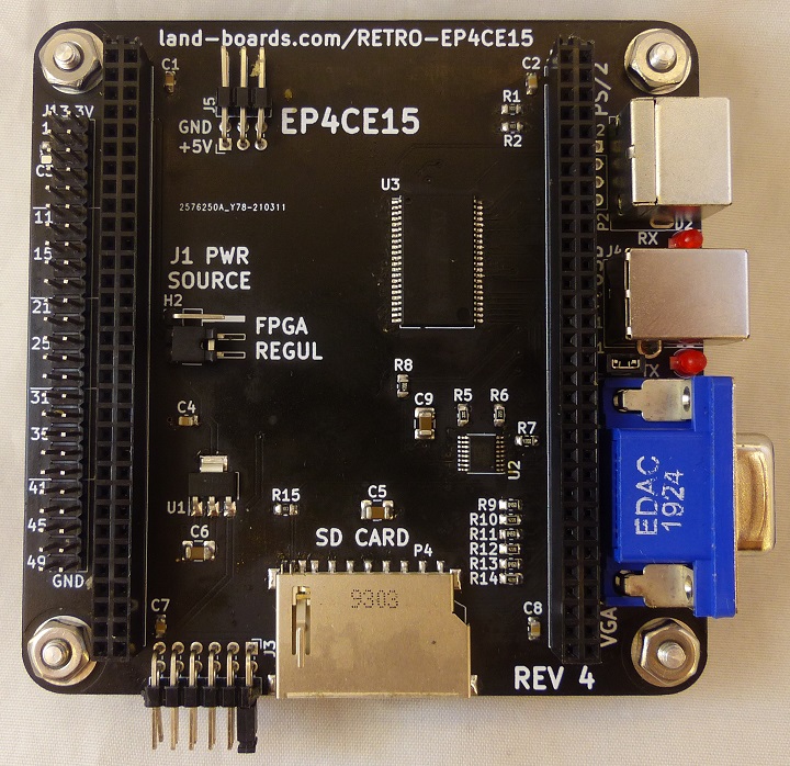
- RETRO-EP4CE15 FPGA base board
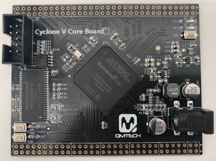
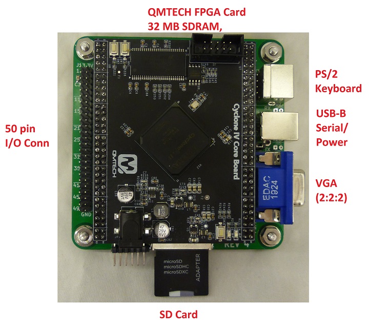
- FPGA card mounted on base board
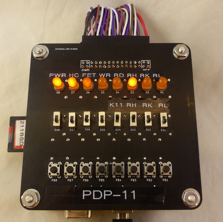
- LEDS-SWITCHES-2 board
Disks (SD card images) that work with PDP2011 build
PDP-11/45 Disks
DOS/BATCH-11 (rk05)
- Switch settings
- RK = Slide Switch 2 (in box)
- DEC BATCH-11/DOS-11
- dos-batch - EC-11-ASDB-D PAL-11R Assembler Programmers Manual May71
- DOS/BATCH-11 (rk05) Disk Image
- Write to SD card - used Balena Etcher (windows) to write SD card
RT-11 4.0 (rk05)
- RK = Slide Switch 2 (in box)
- Wikipedia article
- RT-11 System User's Guide 1977
- RT–11 System Message Manual
- Release History
- Digital’s RT-11 File System
- RT-11 4.0 (rk05) Disk Image
- Write to SD card - used Balena Etcher (windows) to write SD card
RT-11FB 4.0 (rk05)
- RK = Slide Switch 2 (in box)
- RT-11FB (Foreground/Background) supported two tasks: a high-priority, non-interactive "Foreground" job, and a low-priority, interactive "Background" job
- RT-11FB 4.0 (rk05)
RT-11 5.4 (rk05)
- RK = Slide Switch 2 (in box)
- RT-11 5.4 (rk05) Disk Image
- Write to SD card - used Balena Etcher (windows) to write SD card
- DIR or DIR/BRIEF
- A tutorial introduction to programming PDP-11 Macro-11 Assembly in RT-11 v5.3
- AA-5281C-TC Introduction to RT-11 v5.1 1983
- AA-5279C-TC-RT-11-5.1 System Users Guide 1983
- AA-M239B-TC-RT-11-5.1 System Utilities Manual 1984
- AA-V027A-TC-PDP11 MACRO-11 Language Reference Manual 1983
- Power-on message similar to:
               RT-11 V5.4F

Installation of RT-11 Version 5.4F is complete and you are now running
RT-11 from your system volume,

Your system volume is your working volume if you have used the
automatic installation (AI) procedure. If you have installed RT-11 using
that procedure. DIGITAL recommends you verify the correct operation of
your system's software using the VERIFY verification procedure.
To do this, enter the command:

                             IND VERIFY

Note that VERIFY should be performed  only after the distribution
media have been backed up.  This was accomplished as part
of automatic installation on  all  RL02,  RX02,  TK50, and  RX50
based systems,   including the  MicroPDP-11 and the Professional
300.  If you have not completed automatic installation, you must
perform a manual backup before using VERIFY.  Note also,  VERIFY
is NOT supported on RX01 diskettes,    DECtape I or II,   or the
Professional 325.

DIGITAL also  recommends  you  read  the  file V5NOTE.TXT, which
contains information  formalized too late to be included  in the
Release Notes.  V5NOTE.TXT can be TYPED or PRINTED.
- Prompt is dot (.)
- datime format
- 01-May-99
- type command
- The type command will show the contents of a file, just like MS-DOS
- RUN command
- Dungeon for example is executed with RUN. I think you have to run .sav files.
- .RUN DUNGEO
- .SAV files can be run
- .RUN DUNGEO
- @ command
- COM files are like batch scripts, and are executed with the @ infront of them.
- .@STARTS.COM
- SHOW command
- This is a very useful command to show some info about the OS.
- .SHOW
UNIX V7 (rl02)
- RL = Slide Switch 1 (in box)
- UNIX V7 (rl02) Disk Image
- Write to SD card - used Balena Etcher (windows) to write SD card
PDP-11/70 disks
211BSD (rp06)
- RP = Slide Switch 3 (in box)
- 211BSD (rp06) Disk Image
- Write to SD card - used Balena Etcher (windows) to write SD card
- Boot screen
Hello, world [t44]: cpu 11/70
boot from rp:
70Boot from xp(0,0,0) at 0176700
: «
: xp(0,0,0)unix
Boot: bootdev=05000 bootcsr=0176700
2.11 BSD UNIX #115: Sat Apr 22 19:07:25 PDT 2000
    sms1@curly.2bsd.com:/usr/src/sys/GENERIC
phys mem  = 3932160
avail mem = 3708224
user mem  = 307200
- Running
- Enter
- At the first '#' prompt the system is in single-user mode. Just enter a ^D to continue the system startup to multi-user mode
- Login: root
- At the end is important to shutdown properly with a halt:
     # {pstat -T}
      49/186 files
      65/208 inodes
      16/150 processes
      11/ 46 texts active,  37 used
       3/135 swapmap entries,  530 kB used, 3649 kB free, 3642 kB max
      33/150 coremap entries, 2599 kB free, 2520 kB max
       1/ 10  ub_map entries,    8    free,    8    max
     # {mount}
     /dev/xp0a on /
     /dev/xp0c on /tmp
     /dev/xp0d on /home
     /dev/xp0e on /usr
     # {halt}
     syncing disks... done
     halting
RSX-11M PLUS 3.0 (rp06)
- RP = Slide Switch 3 (in box)
- RSX-11M PLUS 3.0 (rp06) Disk Image
- Write to SD card - used Balena Etcher (windows) to write SD card
Other Disk Images
- RL images are in chunks of 256 bytes, and require inserting 256 bytes padding after each of those chunks
- sdfmt converts files to 256 out of 512 bytes - Runs under Linux
- System Disk Images
- Disk Images
- W11 OS Disk sets - Well documented
- OS Kits
Other PDP2011 Builds
- PDP2011 by Sytse van Slooten - the original project
- David Richards PDP-11 Build on A-ESTF V2 EP4CE22 Board
- W11 PDP-11/70 Project
Software
Documentation
- PDP-11 Processor Handbook 1981 - on BitSavers
- PDP-11/45 System User's Manual
- PDP-11/70 Processor Handbook
PDP-11 Front Panel
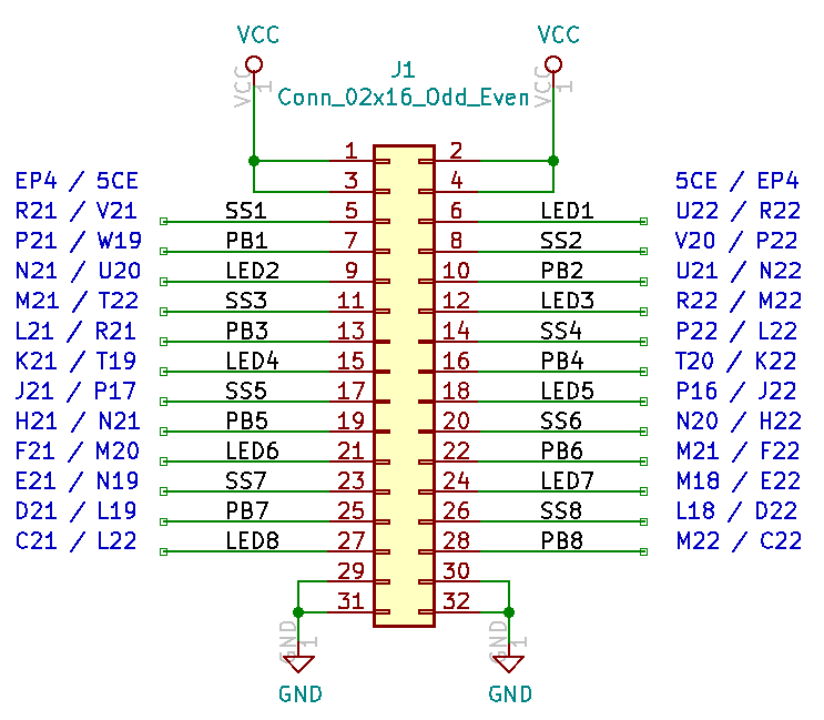
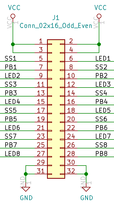
Front Panel Pins Directly Mapped to RETRO-EP4CE15
Front Panel J1
- Front Panel Card cables up to 50-pin connector on RETRO-EP4CE15 Card
- 32-pin connector
- Wiring "flipped" and directly in order
- Note extra ground/power pins on the Front Panel card
I/O Connector (5CEFA2F23 FPGA Card pin numbers)
| Function | Marking | 5CEFA2 FPGA Pin |
|---|---|---|
| resetbtn pushbutton | PB8 | PIN_M22 |
| PWR LED | D8 | PIN_L22 |
| sdHC LED | D7 | PIN_M18 |
| FETch LED | D6 | PIN_M20 |
| sdWR LED | D5 | PIN_P16 |
| sdRD LED | D4 | PIN_T19 |
| RH Drive (rp) LED | D3 | PIN_R22 |
| RK Drive LED | D2 | PIN_U20 |
| RL Drive LED | D1 | PIN_U22 |
| K11 (tty1) Slide switch | SS4 | PIN_P22 |
| RH Drive (rp) (UP) Slide switch | SS3 | PIN_T22 |
| RK Drive (UP) Slide switch | SS2 | PIN_V20 |
| RL Drive (UP) Slide switch | SS1 | PIN_V21 |
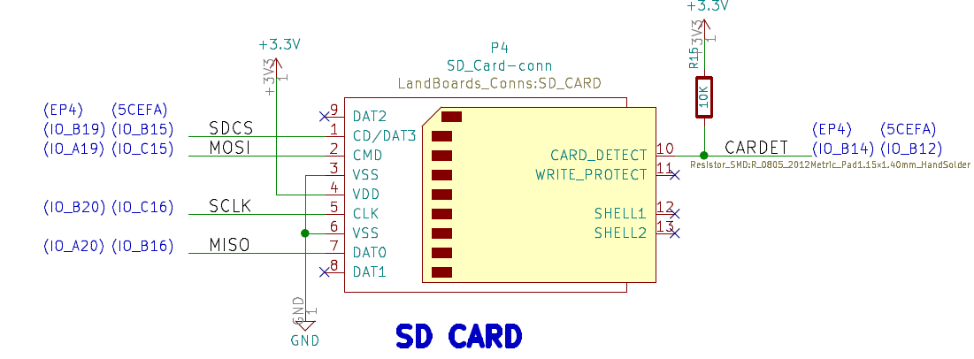
P4 - SD Card (5CEFA2F23 FPGA pin numbers)
- This build works with SD and SD/HC cards
- SDCS = U7-57 = PIN_B15
- MOSI = U7-58 = PIN_C15
- SCK = U7-59 = PIN_C16
- MISO = U7-60 = PIN_B16
- SD_DETECT - PIN_B12
MultiComp in Box Pins Mapping
Slide Switches/Reset Pushbutton
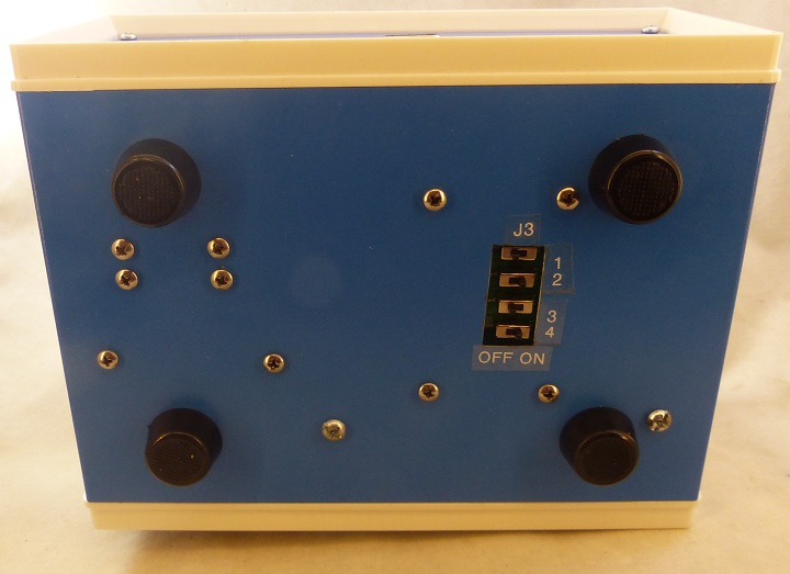
- Slide switches are on the bottom of the box
- Slide switches are on the bottom of the box
- PIN_L17 - Slide Switch 1 (top switch) - RL Drive select
- PIN_K17 - Slide Switch 2 - RK Drive select
- PIN_K22 - Slide Switch 3 - RH/RP Drive select
- PIN_K21 - Slide Switch 4 (bottom switch)
- Reset switch is on the front of the boz
- PIN_N16 - Reset Switch
SD Card
- External SD Card
- Install J3 on SD Card
- Runs card off 3.3V
- NO5V jumper installed
| J1 PIN | SIGNAL | COLOR | SD PIN | FPGA Pin | DIR |
|---|---|---|---|---|---|
| 2 | 3.3V | ORG | 7 | VREG 3.3V | OUT (PWR) |
| 45 | sdSCLK | GRY | 3 | PIN_L19 | OUT |
| 46 | sdMISO | BLU | 2 | PIN_L18 | IN |
| 47 | sdMOSI | WHT | 4 | PIN_L22 | OUT |
| 48 | sdCS | VIO | 5 | PIN_M22 | OUT |
| 49 | GND | GRN | 1 | GND | OUT (PWR) |
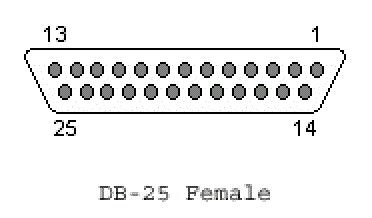
MultiComp DB-25 Pinout
- MultiComp in a Box has a DB-25 Female connector
- DB25-02 - DB-25 adapter with Male connector
- Front panel card has 32-pin connector
- Dupont pin cable connects the two cards
- DB-25F on MultiComp in a Box as viewed from front of box
Front Panel Pinout
MultiComp in Box Front Panel Cabling
| DB25F | P1(DB25-02) | FPGA J1 | Signal | SW-J1 | FPGA | DB25F | P1(DB25-02) | FPGA J1 | Signal | SW-J1 | FPGA | |
|---|---|---|---|---|---|---|---|---|---|---|---|---|
| 1 | 25 | 26 | NC | |||||||||
| 2 | 23 | GND | 32 | 14 | 24 | GND | ||||||
| 3 | 21 | 44 | SS1 | 5 | PIN_M18 | 15 | 22 | 43 | SS2 | 8 | PIN_N19 | |
| 4 | 19 | 42 | SS3 | 11 | PIN_M21 | 16 | 20 | 41 | SS4 | 14 | PIN_M20 | |
| 5 | 17 | 40 | N/C | PIN_N20 | 17 | 18 | 39 | N/C | PIN_N21 | |||
| 6 | 15 | 38 | LED1 | 6 | PIN_P16 | 18 | 16 | 37 | LED2 | 9 | PIN_P17 | |
| 7 | 13 | 36 | LED3 | 12 | PIN_T20 | 19 | 14 | 35 | LED4 | 15 | PIN_T19 | |
| 8 | 11 | 34 | LED5 | 18 | PIN_P22 | 20 | 12 | 33 | LED6 | 21 | PIN_R21 | |
| 9 | 9 | 32 | LED7 | 24 | PIN_R22 | 21 | 10 | 31 | LED8 | 27 | PIN_T22 | |
| 10 | 7 | 30 | PB8 | 28 | PIN_U21 | 22 | 8 | 29 | PIN_U20 | |||
| 11 | 5 | 23 | 6 | |||||||||
| 12 | 3 | 24 | 4 | |||||||||
| 13 | 1 | +3.3V | 2 | 25 | 2 | +3.3V |
Connectors on RETROEP4-CE15 Card
P1 - VGA
- videoR0 = U8-49 = PIN_E12
- videoR1 = U8-50 = PIN_D12
- videoG0 = U8-51 = PIN_D13
- videoG1 = U8-52 = PIN_C13
- videoB0 = U8-53 = PIN_B13
- videoB1 = U8-54 = PIN_A13
- hSync = U8-55 = PIN_A15
- vSync = U8-56 = PIN_A14
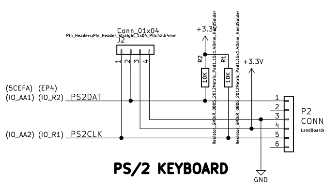
P2 - PS/2 Keyboard
- PS2DAT = U7-8 = PIN_BANK_2A_AA1
- PS2CLK = U7-8 = PIN_NANK_2A_AA2
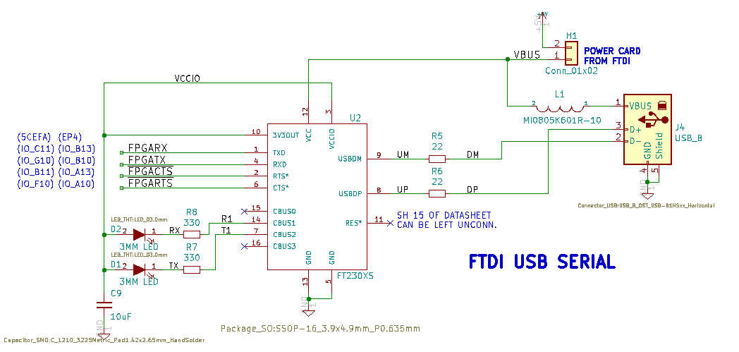
P3 - Serial Ports - I/O connector
- fpgaRx1 (in) = PIN_C11
- fpgaTx1 (out) = PIN_G10
- fpgaRts1 = U7-44 = PIN_F10
- fpgaCts1 = U7-46 = PIN_B11
IO conn
- Second serial port on I/O connector
- rx2 (in) = PIN_M18
- tx2 (out) = PIN_L19
- rts2 (out) = PIN_N19
- cts2 (in) = PIN_M21
J4 - USB-B B (5CEFA2F23 FPGA Card pin numbers) Serial Port
- On-board FT230X FTDI USB to Serial
FPGA Resources
- Uses > 80% of the ALMs
PDP-11/45
- No Front Panel
- In MultiComp Box
+-------------------------------------------------------------------------------+
; Fitter Summary                                                                ;
+---------------------------------+---------------------------------------------+
; Fitter Status                   ; Successful - Sun May  1 13:02:25 2022       ;
; Quartus Prime Version           ; 21.1.0 Build 842 10/21/2021 SJ Lite Edition ;
; Revision Name                   ; top                                         ;
; Top-level Entity Name           ; top                                         ;
; Family                          ; Cyclone V                                   ;
; Device                          ; 5CEFA2F23I7                                 ;
; Timing Models                   ; Final                                       ;
; Logic utilization (in ALMs)     ; 7,797 / 9,430 ( 83 % )                      ;
; Total registers                 ; 6002                                        ;
; Total pins                      ; 68 / 224 ( 30 % )                           ;
; Total virtual pins              ; 0                                           ;
; Total block memory bits         ; 180,224 / 1,802,240 ( 10 % )                ;
; Total RAM Blocks                ; 25 / 176 ( 14 % )                           ;
; Total DSP Blocks                ; 1 / 25 ( 4 % )                              ;
; Total HSSI RX PCSs              ; 0                                           ;
; Total HSSI PMA RX Deserializers ; 0                                           ;
; Total HSSI TX PCSs              ; 0                                           ;
; Total HSSI PMA TX Serializers   ; 0                                           ;
; Total PLLs                      ; 1 / 4 ( 25 % )                              ;
; Total DLLs                      ; 0 / 4 ( 0 % )                               ;
+---------------------------------+---------------------------------------------+
PDP-11/70
- Front Panel
- In MultiComp Box
+-------------------------------------------------------------------------------+
; Fitter Summary                                                                ;
+---------------------------------+---------------------------------------------+
; Fitter Status                   ; Successful - Sat Apr 30 19:30:51 2022       ;
; Quartus Prime Version           ; 21.1.0 Build 842 10/21/2021 SJ Lite Edition ;
; Revision Name                   ; top                                         ;
; Top-level Entity Name           ; top                                         ;
; Family                          ; Cyclone V                                   ;
; Device                          ; 5CEFA2F23I7                                 ;
; Timing Models                   ; Final                                       ;
; Logic utilization (in ALMs)     ; 7,809 / 9,430 ( 83 % )                      ;
; Total registers                 ; 6016                                        ;
; Total pins                      ; 76 / 224 ( 34 % )                           ;
; Total virtual pins              ; 0                                           ;
; Total block memory bits         ; 180,224 / 1,802,240 ( 10 % )                ;
; Total RAM Blocks                ; 25 / 176 ( 14 % )                           ;
; Total DSP Blocks                ; 1 / 25 ( 4 % )                              ;
; Total HSSI RX PCSs              ; 0                                           ;
; Total HSSI PMA RX Deserializers ; 0                                           ;
; Total HSSI TX PCSs              ; 0                                           ;
; Total HSSI PMA TX Serializers   ; 0                                           ;
; Total PLLs                      ; 1 / 4 ( 25 % )                              ;
; Total DLLs                      ; 0 / 4 ( 0 % )                               ;
+---------------------------------+---------------------------------------------+
External Resources
- PDP2011 by Sytse van Slooten
- Active as of 2021-11
- David J Richards PDP-11 Build - copied and adapted from pdp2011 by Sytse van Slooten
- PDP-11 on BitSavers
- Scott L Baker PDP11-SOC
- PDP-11/20 CPU
- UART + Timer + I/O Ports coded in VHDL
- 8KB RAM
- Implemented on the Lattice iCE40-hx8k dev board
- w11: PDP 11/70 CPU and SoC
- PDP-11/70 CPU with memory management unit, but without floating point unit,
- Quick start Guide
- OS Kits (Disk Images)
- Guide to run operating system images on w11a systems
- Guide to install and build w11a systems, test benches and support software
Programming the FPGA EEPROM (5CEFA2F23 FPGA)
- File
- Convert Programming File
- Configuration Device = MT25QL128
- Mode = Active Serial
- Programming File Type: *.jic
- Advanced = Check both Disables...
- Select Flash Loader
- Add Device = Cyclone V and 5CEFA2
- Select SOF Data
- Select Add File and select the .sof file
- Generate
- In Tools, Programmer
- Mode: JTAG
- Add file and select the .jic file
- Select Program/Configure
- Takes a while to program
- Press button near VGA
Pin Lists
Pin List Standalone with Front Panel
- With LEDS-SWITCHES-2 card
| To | Direction | Location | I/O Standard | Pull-Up |
|---|---|---|---|---|
| clkin | Input | PIN_M9 | 3.3-V LVTTL | |
| cts1 | Input | PIN_B11 | 3.3-V LVTTL | |
| dram_addr[0] | Output | PIN_P8 | 3.3-V LVTTL | |
| dram_addr[1] | Output | PIN_P7 | 3.3-V LVTTL | |
| dram_addr[10] | Output | PIN_R6 | 3.3-V LVTTL | |
| dram_addr[11] | Output | PIN_T9 | 3.3-V LVTTL | |
| dram_addr[12] | Output | PIN_Y9 | 3.3-V LVTTL | |
| dram_addr[2] | Output | PIN_N8 | 3.3-V LVTTL | |
| dram_addr[3] | Output | PIN_N6 | 3.3-V LVTTL | |
| dram_addr[4] | Output | PIN_U6 | 3.3-V LVTTL | |
| dram_addr[5] | Output | PIN_U7 | 3.3-V LVTTL | |
| dram_addr[6] | Output | PIN_V6 | 3.3-V LVTTL | |
| dram_addr[7] | Output | PIN_U8 | 3.3-V LVTTL | |
| dram_addr[8] | Output | PIN_T8 | 3.3-V LVTTL | |
| dram_addr[9] | Output | PIN_W8 | 3.3-V LVTTL | |
| dram_ba_0 | Output | PIN_T7 | 3.3-V LVTTL | |
| dram_ba_1 | Output | PIN_P9 | 3.3-V LVTTL | |
| dram_cas_n | Output | PIN_AA7 | 3.3-V LVTTL | |
| dram_cke | Output | PIN_V9 | 3.3-V LVTTL | |
| dram_clk | Output | PIN_AB11 | 3.3-V LVTTL | |
| dram_cs_n | Output | PIN_AB5 | 3.3-V LVTTL | |
| dram_dq[0] | Bidir | PIN_AA12 | 3.3-V LVTTL | |
| dram_dq[1] | Bidir | PIN_Y11 | 3.3-V LVTTL | |
| dram_dq[10] | Bidir | PIN_U11 | 3.3-V LVTTL | |
| dram_dq[11] | Bidir | PIN_R10 | 3.3-V LVTTL | |
| dram_dq[12] | Bidir | PIN_R11 | 3.3-V LVTTL | |
| dram_dq[13] | Bidir | PIN_U12 | 3.3-V LVTTL | |
| dram_dq[14] | Bidir | PIN_R12 | 3.3-V LVTTL | |
| dram_dq[15] | Bidir | PIN_P12 | 3.3-V LVTTL | |
| dram_dq[2] | Bidir | PIN_AA10 | 3.3-V LVTTL | |
| dram_dq[3] | Bidir | PIN_AB10 | 3.3-V LVTTL | |
| dram_dq[4] | Bidir | PIN_Y10 | 3.3-V LVTTL | |
| dram_dq[5] | Bidir | PIN_AA9 | 3.3-V LVTTL | |
| dram_dq[6] | Bidir | PIN_AB8 | 3.3-V LVTTL | |
| dram_dq[7] | Bidir | PIN_AA8 | 3.3-V LVTTL | |
| dram_dq[8] | Bidir | PIN_U10 | 3.3-V LVTTL | |
| dram_dq[9] | Bidir | PIN_T10 | 3.3-V LVTTL | |
| dram_ldqm | Output | PIN_AB7 | 3.3-V LVTTL | |
| dram_ras_n | Output | PIN_AB6 | 3.3-V LVTTL | |
| dram_udqm | Output | PIN_V10 | 3.3-V LVTTL | |
| dram_we_n | Output | PIN_W9 | 3.3-V LVTTL | |
| i_PB[1] | Input | PIN_W19 | 3.3-V LVTTL | |
| i_PB[2] | Input | PIN_U21 | 3.3-V LVTTL | |
| i_PB[3] | Input | PIN_R21 | 3.3-V LVTTL | |
| i_PB[4] | Input | PIN_T20 | 3.3-V LVTTL | |
| i_PB[5] | Input | PIN_N21 | 3.3-V LVTTL | |
| i_PB[6] | Input | PIN_M21 | 3.3-V LVTTL | |
| i_PB[7] | Input | PIN_L19 | 3.3-V LVTTL | |
| i_PB[8] | Input | PIN_M22 | 3.3-V LVTTL | |
| i_SS[1] | Input | PIN_V21 | 3.3-V LVTTL | |
| i_SS[2] | Input | PIN_V20 | 3.3-V LVTTL | |
| i_SS[3] | Input | PIN_T22 | 3.3-V LVTTL | |
| i_SS[4] | Input | PIN_P22 | 3.3-V LVTTL | |
| i_SS[5] | Input | PIN_P17 | 3.3-V LVTTL | |
| i_SS[6] | Input | PIN_N20 | 3.3-V LVTTL | |
| i_SS[7] | Input | PIN_N19 | 3.3-V LVTTL | |
| i_SS[8] | Input | PIN_L18 | 3.3-V LVTTL | |
| o_LED[1] | Output | PIN_U22 | 3.3-V LVTTL | |
| o_LED[2] | Output | PIN_U20 | 3.3-V LVTTL | |
| o_LED[3] | Output | PIN_R22 | 3.3-V LVTTL | |
| o_LED[4] | Output | PIN_T19 | 3.3-V LVTTL | |
| o_LED[5] | Output | PIN_P16 | 3.3-V LVTTL | |
| o_LED[6] | Output | PIN_M20 | 3.3-V LVTTL | |
| o_LED[7] | Output | PIN_M18 | 3.3-V LVTTL | |
| o_LED[8] | Output | PIN_L22 | 3.3-V LVTTL | |
| ps2k_c | Input | PIN_AA2 | 3.3-V LVTTL | |
| ps2k_d | Input | PIN_AA1 | 3.3-V LVTTL | |
| rts1 | Output | PIN_F10 | 3.3-V LVTTL | |
| rx1 | Input | PIN_C11 | 3.3-V LVTTL | |
| sdcard_cs | Output | PIN_B15 | 3.3-V LVTTL | |
| sdcard_miso | Input | PIN_B16 | 3.3-V LVTTL | |
| sdcard_mosi | Output | PIN_C15 | 3.3-V LVTTL | |
| sdcard_sclk | Output | PIN_C16 | 3.3-V LVTTL | |
| tx1 | Output | PIN_G10 | 3.3-V LVTTL | |
| vgab[0] | Output | PIN_B13 | 3.3-V LVTTL | |
| vgab[1] | Output | PIN_A13 | 3.3-V LVTTL | |
| vgag[0] | Output | PIN_D13 | 3.3-V LVTTL | |
| vgag[1] | Output | PIN_C13 | 3.3-V LVTTL | |
| vgah | Output | PIN_A15 | 3.3-V LVTTL | |
| vgar[0] | Output | PIN_E12 | 3.3-V LVTTL | |
| vgar[1] | Output | PIN_D12 | 3.3-V LVTTL | |
| vgav | Output | PIN_A14 | 3.3-V LVTTL | |
| xu_cs | Output | 3.3-V LVTTL | ||
| xu_debug_tx | Output | 3.3-V LVTTL | ||
| xu_miso | Input | 3.3-V LVTTL | ||
| xu_mosi | Output | 3.3-V LVTTL | ||
| xu_sclk | Output | 3.3-V LVTTL |
qsf Standalone file with Front Panel
set_global_assignment -name FAMILY "Cyclone V"
set_global_assignment -name DEVICE 5CEFA2F23I7
set_global_assignment -name TOP_LEVEL_ENTITY top
set_global_assignment -name ORIGINAL_QUARTUS_VERSION 9.0
set_global_assignment -name PROJECT_CREATION_TIME_DATE "23:14:32  MARCH 19, 2009"
set_global_assignment -name LAST_QUARTUS_VERSION "21.1.0 Lite Edition"
set_global_assignment -name STRATIX_DEVICE_IO_STANDARD "3.3-V LVTTL"
set_global_assignment -name CYCLONEII_RESERVE_NCEO_AFTER_CONFIGURATION "USE AS REGULAR IO"
set_global_assignment -name RESERVE_ASDO_AFTER_CONFIGURATION "AS INPUT TRI-STATED"
set_global_assignment -name MIN_CORE_JUNCTION_TEMP "-40"
set_global_assignment -name MAX_CORE_JUNCTION_TEMP 100
set_global_assignment -name POWER_PRESET_COOLING_SOLUTION "23 MM HEAT SINK WITH 200 LFPM AIRFLOW"
set_global_assignment -name POWER_BOARD_THERMAL_MODEL "NONE (CONSERVATIVE)"
# Clock
set_location_assignment PIN_M9 -to clkin
# Pushbuttons on LEDS-SWITCHES-2 card
set_location_assignment PIN_M22 -to i_PB[8]
set_location_assignment PIN_L19 -to i_PB[7]
set_location_assignment PIN_M21 -to i_PB[6]
set_location_assignment PIN_N21 -to i_PB[5]
set_location_assignment PIN_T20 -to i_PB[4]
set_location_assignment PIN_R21 -to i_PB[3]
set_location_assignment PIN_U21 -to i_PB[2]
set_location_assignment PIN_W19 -to i_PB[1]
set_location_assignment PIN_L18 -to i_SS[8]
set_location_assignment PIN_N19 -to i_SS[7]
set_location_assignment PIN_N20 -to i_SS[6]
set_location_assignment PIN_P17 -to i_SS[5]
set_location_assignment PIN_P22 -to i_SS[4]
set_location_assignment PIN_T22 -to i_SS[3]
set_location_assignment PIN_V20 -to i_SS[2]
set_location_assignment PIN_V21 -to i_SS[1]
# LEDs on LEDS-SWITCHES-2 card
set_location_assignment PIN_L22 -to o_LED[8]
set_location_assignment PIN_M18 -to o_LED[7]
set_location_assignment PIN_M20 -to o_LED[6]
set_location_assignment PIN_P16 -to o_LED[5]
set_location_assignment PIN_T19 -to o_LED[4]
set_location_assignment PIN_R22 -to o_LED[3]
set_location_assignment PIN_U20 -to o_LED[2]
set_location_assignment PIN_U22 -to o_LED[1]
# SDRAM
set_location_assignment PIN_Y9 -to dram_addr[12]
set_location_assignment PIN_T9 -to dram_addr[11]
set_location_assignment PIN_R6 -to dram_addr[10]
set_location_assignment PIN_W8 -to dram_addr[9]
set_location_assignment PIN_T8 -to dram_addr[8]
set_location_assignment PIN_U8 -to dram_addr[7]
set_location_assignment PIN_V6 -to dram_addr[6]
set_location_assignment PIN_U7 -to dram_addr[5]
set_location_assignment PIN_U6 -to dram_addr[4]
set_location_assignment PIN_N6 -to dram_addr[3]
set_location_assignment PIN_N8 -to dram_addr[2]
set_location_assignment PIN_P7 -to dram_addr[1]
set_location_assignment PIN_P8 -to dram_addr[0]
set_location_assignment PIN_P9 -to dram_ba_1
set_location_assignment PIN_T7 -to dram_ba_0
set_location_assignment PIN_AA7 -to dram_cas_n
set_location_assignment PIN_V9 -to dram_cke
set_location_assignment PIN_AB11 -to dram_clk
set_location_assignment PIN_AB5 -to dram_cs_n
set_location_assignment PIN_P12 -to dram_dq[15]
set_location_assignment PIN_R12 -to dram_dq[14]
set_location_assignment PIN_U12 -to dram_dq[13]
set_location_assignment PIN_R11 -to dram_dq[12]
set_location_assignment PIN_R10 -to dram_dq[11]
set_location_assignment PIN_U11 -to dram_dq[10]
set_location_assignment PIN_T10 -to dram_dq[9]
set_location_assignment PIN_U10 -to dram_dq[8]
set_location_assignment PIN_AA8 -to dram_dq[7]
set_location_assignment PIN_AB8 -to dram_dq[6]
set_location_assignment PIN_AA9 -to dram_dq[5]
set_location_assignment PIN_Y10 -to dram_dq[4]
set_location_assignment PIN_AB10 -to dram_dq[3]
set_location_assignment PIN_AA10 -to dram_dq[2]
set_location_assignment PIN_Y11 -to dram_dq[1]
set_location_assignment PIN_AA12 -to dram_dq[0]
set_location_assignment PIN_V10 -to dram_udqm
set_location_assignment PIN_AB7 -to dram_ldqm
set_location_assignment PIN_AB6 -to dram_ras_n
set_location_assignment PIN_W9 -to dram_we_n
# Serial port (USB-to-Serial)
set_location_assignment PIN_C11 -to rx1
set_location_assignment PIN_G10 -to tx1
set_location_assignment PIN_F10 -to rts1
set_location_assignment PIN_B11 -to cts1
# Second serial port
# SD Card
set_location_assignment PIN_C16 -to sdcard_sclk
set_location_assignment PIN_B15 -to sdcard_cs
set_location_assignment PIN_B16 -to sdcard_miso
set_location_assignment PIN_C15 -to sdcard_mosi
# Ethernet
# PS/2 Keyboard
set_location_assignment PIN_AA2 -to ps2k_c
set_location_assignment PIN_AA1 -to ps2k_d
# Video
set_location_assignment PIN_E12 -to vgar[0]
set_location_assignment PIN_D12 -to vgar[1]
set_location_assignment PIN_B13 -to vgab[0]
set_location_assignment PIN_A13 -to vgab[1]
set_location_assignment PIN_D13 -to vgag[0]
set_location_assignment PIN_C13 -to vgag[1]
set_location_assignment PIN_A15 -to vgah
set_location_assignment PIN_A14 -to vgav
Pin List Standalone
qsf file Standalone
set_global_assignment -name FAMILY "Cyclone V"
set_global_assignment -name DEVICE 5CEFA2F23I7
set_global_assignment -name TOP_LEVEL_ENTITY top
set_global_assignment -name ORIGINAL_QUARTUS_VERSION 9.0
set_global_assignment -name PROJECT_CREATION_TIME_DATE "23:14:32  MARCH 19, 2009"
set_global_assignment -name LAST_QUARTUS_VERSION "21.1.0 Lite Edition"
set_global_assignment -name STRATIX_DEVICE_IO_STANDARD "3.3-V LVTTL"
set_global_assignment -name CYCLONEII_RESERVE_NCEO_AFTER_CONFIGURATION "USE AS REGULAR IO"
set_global_assignment -name RESERVE_ASDO_AFTER_CONFIGURATION "AS INPUT TRI-STATED"
set_location_assignment PIN_M9 -to clkin
set_location_assignment PIN_M22 -to resetbtn
set_instance_assignment -name WEAK_PULL_UP_RESISTOR ON -to resetbtn
# Control switches
# Jumpers on front edge
# SDRAM
set_location_assignment PIN_Y9 -to dram_addr[12]
set_location_assignment PIN_T9 -to dram_addr[11]
set_location_assignment PIN_R6 -to dram_addr[10]
set_location_assignment PIN_W8 -to dram_addr[9]
set_location_assignment PIN_T8 -to dram_addr[8]
set_location_assignment PIN_U8 -to dram_addr[7]
set_location_assignment PIN_V6 -to dram_addr[6]
set_location_assignment PIN_U7 -to dram_addr[5]
set_location_assignment PIN_U6 -to dram_addr[4]
set_location_assignment PIN_N6 -to dram_addr[3]
set_location_assignment PIN_N8 -to dram_addr[2]
set_location_assignment PIN_P7 -to dram_addr[1]
set_location_assignment PIN_P8 -to dram_addr[0]
set_location_assignment PIN_P9 -to dram_ba_1
set_location_assignment PIN_T7 -to dram_ba_0
set_location_assignment PIN_AA7 -to dram_cas_n
set_location_assignment PIN_V9 -to dram_cke
set_location_assignment PIN_AB11 -to dram_clk
set_location_assignment PIN_AB5 -to dram_cs_n
set_location_assignment PIN_P12 -to dram_dq[15]
set_location_assignment PIN_R12 -to dram_dq[14]
set_location_assignment PIN_U12 -to dram_dq[13]
set_location_assignment PIN_R11 -to dram_dq[12]
set_location_assignment PIN_R10 -to dram_dq[11]
set_location_assignment PIN_U11 -to dram_dq[10]
set_location_assignment PIN_T10 -to dram_dq[9]
set_location_assignment PIN_U10 -to dram_dq[8]
set_location_assignment PIN_AA8 -to dram_dq[7]
set_location_assignment PIN_AB8 -to dram_dq[6]
set_location_assignment PIN_AA9 -to dram_dq[5]
set_location_assignment PIN_Y10 -to dram_dq[4]
set_location_assignment PIN_AB10 -to dram_dq[3]
set_location_assignment PIN_AA10 -to dram_dq[2]
set_location_assignment PIN_Y11 -to dram_dq[1]
set_location_assignment PIN_AA12 -to dram_dq[0]
set_location_assignment PIN_V10 -to dram_udqm
set_location_assignment PIN_AB7 -to dram_ldqm
set_location_assignment PIN_AB6 -to dram_ras_n
set_location_assignment PIN_W9 -to dram_we_n
# Serial port (USB-to-Serial)
set_location_assignment PIN_L19 -to rx1
set_location_assignment PIN_L18 -to tx1
set_location_assignment PIN_M18 -to rts1
set_location_assignment PIN_N19 -to cts1
# Second serial port
# SD Card
set_location_assignment PIN_C16 -to sdcard_sclk
set_location_assignment PIN_B15 -to sdcard_cs
set_location_assignment PIN_B16 -to sdcard_miso
set_location_assignment PIN_C15 -to sdcard_mosi
# Seven segment display (on J1)
# Ethernet
set_location_assignment PIN_T20 -to xu_cs
set_location_assignment PIN_P17 -to xu_debug_tx
set_location_assignment PIN_P16 -to xu_miso
set_location_assignment PIN_N21 -to xu_mosi
set_location_assignment PIN_N20 -to xu_sclk
# PS/2 Keyboard
set_location_assignment PIN_AA2 -to ps2k_c
set_location_assignment PIN_AA1 -to ps2k_d
# Video
set_location_assignment PIN_A15 -to vgah
set_location_assignment PIN_A14 -to vgav

set_global_assignment -name PARTITION_NETLIST_TYPE SOURCE -section_id Top
set_global_assignment -name PARTITION_FITTER_PRESERVATION_LEVEL PLACEMENT_AND_ROUTING -section_id Top
set_global_assignment -name PARTITION_COLOR 16764057 -section_id Top

set_global_assignment -name MIN_CORE_JUNCTION_TEMP "-40"
set_global_assignment -name MAX_CORE_JUNCTION_TEMP 100
set_global_assignment -name POWER_PRESET_COOLING_SOLUTION "23 MM HEAT SINK WITH 200 LFPM AIRFLOW"
set_global_assignment -name POWER_BOARD_THERMAL_MODEL "NONE (CONSERVATIVE)"
set_location_assignment PIN_E12 -to vgar[0]
set_location_assignment PIN_D12 -to vgar[1]
set_location_assignment PIN_B13 -to vgab[0]
set_location_assignment PIN_A13 -to vgab[1]
set_location_assignment PIN_D13 -to vgag[0]
set_location_assignment PIN_C13 -to vgag[1]
set_location_assignment PIN_L17 -to sw[0]
set_location_assignment PIN_K17 -to sw[1]
set_location_assignment PIN_K22 -to sw[2]
set_location_assignment PIN_K21 -to sw[3]
set_location_assignment PIN_M16 -to sw[4]
set_location_assignment PIN_N16 -to sw[5]
set_location_assignment PIN_R21 -to greenled[0]
set_location_assignment PIN_P22 -to greenled[1]
set_location_assignment PIN_T22 -to greenled[2]
set_location_assignment PIN_R22 -to greenled[3]
set_location_assignment PIN_U20 -to greenled[4]
set_global_assignment -name VHDL_FILE ../vgacr.vhd
set_global_assignment -name VHDL_FILE ../vga.vhd
set_global_assignment -name VHDL_FILE ../vt.vhd
set_global_assignment -name VHDL_FILE ../ps2.vhd
set_global_assignment -name VHDL_FILE ../vgafont.vhd
set_global_assignment -name VHDL_FILE ../vtbrt42.vhd
set_global_assignment -name VHDL_FILE ../sdspi.vhd
set_global_assignment -name VHDL_FILE ../mnckw.vhd
set_global_assignment -name VHDL_FILE ../mncdo.vhd
set_global_assignment -name VHDL_FILE ../mncdi.vhd
set_global_assignment -name VHDL_FILE ../mncad.vhd
set_global_assignment -name VHDL_FILE ../mncaa.vhd
set_global_assignment -name VHDL_FILE ../m9312h47.vhd
set_global_assignment -name VHDL_FILE ../m9312l47.vhd
set_global_assignment -name VHDL_FILE ../dr11c.vhd
set_global_assignment -name VHDL_FILE ../panelos.vhd
set_global_assignment -name VHDL_FILE ../paneldriver.vhd
set_global_assignment -name VHDL_FILE ../paneldb.vhd
set_global_assignment -name VHDL_FILE ../xubrt45.vhd
set_global_assignment -name VHDL_FILE ../xubm.vhd
set_global_assignment -name VHDL_FILE ../xubl.vhd
set_global_assignment -name VHDL_FILE ../xu.vhd
set_global_assignment -name VHDL_FILE ../rh11.vhd
set_global_assignment -name VHDL_FILE ../kl11.vhd
set_global_assignment -name VHDL_FILE ../rk11.vhd
set_global_assignment -name VHDL_FILE ../unibus.vhd
set_global_assignment -name VHDL_FILE ../cr.vhd
set_global_assignment -name VHDL_FILE ../rl11.vhd
set_global_assignment -name VHDL_FILE ../mmu.vhd
set_global_assignment -name VHDL_FILE ../kw11l.vhd
set_global_assignment -name VHDL_FILE ../fpuregs.vhd
set_global_assignment -name VHDL_FILE ../csdr.vhd
set_global_assignment -name VHDL_FILE ../cpuregs.vhd
set_global_assignment -name VHDL_FILE ../cpu.vhd
set_global_assignment -name VHDL_FILE top.vhd
set_global_assignment -name VHDL_FILE ssegdecoder.vhd
set_global_assignment -name CDF_FILE top.cdf
set_global_assignment -name QIP_FILE pll.qip
set_instance_assignment -name PARTITION_HIERARCHY root_partition -to | -section_id Top
Pin List in MultiComp Box
| To | Direction | Location | Pull-Up |
|---|---|---|---|
| clkin | Input | PIN_M9 | |
| cts1 | Input | PIN_B11 | on |
| dram_addr[12] | Output | PIN_Y9 | |
| dram_addr[11] | Output | PIN_T9 | |
| dram_addr[10] | Output | PIN_R6 | |
| dram_addr[9] | Output | PIN_W8 | |
| dram_addr[8] | Output | PIN_T8 | |
| dram_addr[7] | Output | PIN_U8 | |
| dram_addr[6] | Output | PIN_V6 | |
| dram_addr[5] | Output | PIN_U7 | |
| dram_addr[4] | Output | PIN_U6 | |
| dram_addr[3] | Output | PIN_N6 | |
| dram_addr[2] | Output | PIN_N8 | |
| dram_addr[1] | Output | PIN_P7 | |
| dram_addr[0] | Output | PIN_P8 | |
| dram_ba_0 | Output | PIN_T7 | |
| dram_ba_1 | Output | PIN_P9 | |
| dram_cas_n | Output | PIN_AA7 | |
| dram_cke | Output | PIN_V9 | |
| dram_clk | Output | PIN_AB11 | |
| dram_cs_n | Output | PIN_AB5 | |
| dram_dq[15] | Bidir | PIN_P12 | |
| dram_dq[14] | Bidir | PIN_R12 | |
| dram_dq[13] | Bidir | PIN_U12 | |
| dram_dq[12] | Bidir | PIN_R11 | |
| dram_dq[11] | Bidir | PIN_R10 | |
| dram_dq[10] | Bidir | PIN_U11 | |
| dram_dq[9] | Bidir | PIN_T10 | |
| dram_dq[8] | Bidir | PIN_U10 | |
| dram_dq[7] | Bidir | PIN_AA8 | |
| dram_dq[6] | Bidir | PIN_AB8 | |
| dram_dq[5] | Bidir | PIN_AA9 | |
| dram_dq[4] | Bidir | PIN_Y10 | |
| dram_dq[3] | Bidir | PIN_AB10 | |
| dram_dq[2] | Bidir | PIN_AA10 | |
| dram_dq[1] | Bidir | PIN_Y11 | |
| dram_dq[0] | Bidir | PIN_AA12 | |
| dram_ldqm | Output | PIN_AB7 | |
| dram_ras_n | Output | PIN_AB6 | |
| dram_udqm | Output | PIN_V10 | |
| dram_we_n | Output | PIN_W9 | |
| i_PB[8] | Input | PIN_N16 | on |
| i_PB[7] | Input | PIN_Y20 | on |
| i_PB[6] | Input | PIN_M21 | on |
| i_PB[5] | Input | PIN_N21 | on |
| i_PB[4] | Input | PIN_T20 | on |
| i_PB[3] | Input | PIN_R21 | on |
| i_PB[2] | Input | PIN_U21 | on |
| i_PB[1] | Input | PIN_W19 | on |
| i_SS[8] | Input | PIN_P22 | on |
| i_SS[7] | Input | PIN_N19 | on |
| i_SS[6] | Input | PIN_N20 | on |
| i_SS[5] | Input | PIN_M16 | on |
| i_SS[4] | Input | PIN_K21 | on |
| i_SS[3] | Input | PIN_K22 | on |
| i_SS[2] | Input | PIN_K17 | on |
| i_SS[1] | Input | PIN_L17 | on |
| o_LED[8] | Output | PIN_P17 | |
| o_LED[7] | Output | PIN_M18 | |
| o_LED[6] | Output | PIN_M20 | |
| o_LED[5] | Output | PIN_P16 | |
| o_LED[4] | Output | PIN_T19 | |
| o_LED[3] | Output | PIN_R22 | |
| o_LED[2] | Output | PIN_U20 | |
| o_LED[1] | Output | PIN_U22 | |
| ps2k_c | Input | PIN_AA2 | on |
| ps2k_d | Input | PIN_AA1 | on |
| rts1 | Output | PIN_F10 | |
| rx1 | Input | PIN_C11 | on |
| sdcard_cs | Output | PIN_M22 | |
| sdcard_miso | Input | PIN_L18 | on |
| sdcard_mosi | Output | PIN_L22 | |
| sdcard_sclk | Output | PIN_L19 | |
| tx1 | Output | PIN_G10 | |
| vgab[1] | Output | PIN_A13 | |
| vgab[0] | Output | PIN_B13 | |
| vgag[1] | Output | PIN_C13 | |
| vgag[0] | Output | PIN_D13 | |
| vgah | Output | PIN_A15 | |
| vgar[1] | Output | PIN_D12 | |
| vgar[0] | Output | PIN_E12 | |
| vgav | Output | PIN_A14 | |
| xu_cs | Output | PIN_AB22 | |
| xu_debug_tx | Output | PIN_AA22 | |
| xu_miso | Input | PIN_Y22 | on |
| xu_mosi | Output | PIN_V20 | |
| xu_sclk | Output | PIN_T22 |
qsf file in MultiComp Box
set_global_assignment -name FAMILY "Cyclone V"
set_global_assignment -name DEVICE 5CEFA2F23I7
set_global_assignment -name TOP_LEVEL_ENTITY top
set_global_assignment -name ORIGINAL_QUARTUS_VERSION 9.0
set_global_assignment -name PROJECT_CREATION_TIME_DATE "23:14:32  MARCH 19, 2009"
set_global_assignment -name LAST_QUARTUS_VERSION "21.1.0 Lite Edition"
set_global_assignment -name STRATIX_DEVICE_IO_STANDARD "3.3-V LVTTL"
set_global_assignment -name CYCLONEII_RESERVE_NCEO_AFTER_CONFIGURATION "USE AS REGULAR IO"
set_global_assignment -name RESERVE_ASDO_AFTER_CONFIGURATION "AS INPUT TRI-STATED"
set_global_assignment -name PARTITION_NETLIST_TYPE SOURCE -section_id Top
set_global_assignment -name PARTITION_FITTER_PRESERVATION_LEVEL PLACEMENT_AND_ROUTING -section_id Top
set_global_assignment -name PARTITION_COLOR 16764057 -section_id Top
set_global_assignment -name MIN_CORE_JUNCTION_TEMP "-40"
set_global_assignment -name MAX_CORE_JUNCTION_TEMP 100
set_global_assignment -name POWER_PRESET_COOLING_SOLUTION "23 MM HEAT SINK WITH 200 LFPM AIRFLOW"
set_global_assignment -name POWER_BOARD_THERMAL_MODEL "NONE (CONSERVATIVE)"
# Clock
set_location_assignment PIN_M9 -to clkin
# Serial port (USB-to-Serial)
set_location_assignment PIN_C11 -to rx1
set_location_assignment PIN_G10 -to tx1
set_location_assignment PIN_F10 -to rts1
set_location_assignment PIN_B11 -to cts1
set_instance_assignment -name WEAK_PULL_UP_RESISTOR ON -to cts1
set_instance_assignment -name WEAK_PULL_UP_RESISTOR ON -to rx1
# Second serial port
# SD Card
set_location_assignment PIN_L19 -to sdcard_sclk
set_location_assignment PIN_M22 -to sdcard_cs
set_location_assignment PIN_L18 -to sdcard_miso
set_instance_assignment -name WEAK_PULL_UP_RESISTOR ON -to sdcard_miso
set_location_assignment PIN_L22 -to sdcard_mosi
# PS/2 Keyboard
set_location_assignment PIN_AA2 -to ps2k_c
set_location_assignment PIN_AA1 -to ps2k_d
set_instance_assignment -name WEAK_PULL_UP_RESISTOR ON -to ps2k_c
set_instance_assignment -name WEAK_PULL_UP_RESISTOR ON -to ps2k_d
# Video
set_location_assignment PIN_A15 -to vgah
set_location_assignment PIN_A14 -to vgav
set_location_assignment PIN_E12 -to vgar[0]
set_location_assignment PIN_D12 -to vgar[1]
set_location_assignment PIN_B13 -to vgab[0]
set_location_assignment PIN_A13 -to vgab[1]
set_location_assignment PIN_D13 -to vgag[0]
set_location_assignment PIN_C13 -to vgag[1]
# LEDs
set_location_assignment PIN_U22 -to o_LED[1]
set_location_assignment PIN_R22 -to o_LED[3]
set_location_assignment PIN_U20 -to o_LED[2]
set_location_assignment PIN_P17 -to o_LED[8]
set_location_assignment PIN_M18 -to o_LED[7]
set_location_assignment PIN_M20 -to o_LED[6]
set_location_assignment PIN_P16 -to o_LED[5]
set_location_assignment PIN_T19 -to o_LED[4]
# Slide Switches
set_location_assignment PIN_L17 -to i_SS[1]
set_location_assignment PIN_K17 -to i_SS[2]
set_location_assignment PIN_K22 -to i_SS[3]
set_location_assignment PIN_K21 -to i_SS[4]
set_location_assignment PIN_M16 -to i_SS[5]
set_location_assignment PIN_N20 -to i_SS[6]
set_location_assignment PIN_N19 -to i_SS[7]
set_location_assignment PIN_P22 -to i_SS[8]
set_instance_assignment -name WEAK_PULL_UP_RESISTOR ON -to i_SS[8]
set_instance_assignment -name WEAK_PULL_UP_RESISTOR ON -to i_SS[7]
set_instance_assignment -name WEAK_PULL_UP_RESISTOR ON -to i_SS[6]
set_instance_assignment -name WEAK_PULL_UP_RESISTOR ON -to i_SS[5]
set_instance_assignment -name WEAK_PULL_UP_RESISTOR ON -to i_SS[4]
set_instance_assignment -name WEAK_PULL_UP_RESISTOR ON -to i_SS[3]
set_instance_assignment -name WEAK_PULL_UP_RESISTOR ON -to i_SS[2]
set_instance_assignment -name WEAK_PULL_UP_RESISTOR ON -to i_SS[1]
set_instance_assignment -name WEAK_PULL_UP_RESISTOR ON -to i_SS
# Pushbuttons
set_location_assignment PIN_W19 -to i_PB[1]
set_location_assignment PIN_U21 -to i_PB[2]
set_location_assignment PIN_R21 -to i_PB[3]
set_location_assignment PIN_T20 -to i_PB[4]
set_location_assignment PIN_N21 -to i_PB[5]
set_location_assignment PIN_M21 -to i_PB[6]
set_location_assignment PIN_Y20 -to i_PB[7]
set_location_assignment PIN_N16 -to i_PB[8]
set_instance_assignment -name WEAK_PULL_UP_RESISTOR ON -to i_PB[1]
set_instance_assignment -name WEAK_PULL_UP_RESISTOR ON -to i_PB[2]
set_instance_assignment -name WEAK_PULL_UP_RESISTOR ON -to i_PB[3]
set_instance_assignment -name WEAK_PULL_UP_RESISTOR ON -to i_PB[4]
set_instance_assignment -name WEAK_PULL_UP_RESISTOR ON -to i_PB[5]
set_instance_assignment -name WEAK_PULL_UP_RESISTOR ON -to i_PB[6]
set_instance_assignment -name WEAK_PULL_UP_RESISTOR ON -to i_PB[7]
set_instance_assignment -name WEAK_PULL_UP_RESISTOR ON -to i_PB[8]
# Ethernet
set_location_assignment PIN_T22 -to xu_sclk
set_location_assignment PIN_V20 -to xu_mosi
set_location_assignment PIN_Y22 -to xu_miso
set_location_assignment PIN_AA22 -to xu_debug_tx
set_location_assignment PIN_AB22 -to xu_cs
set_instance_assignment -name WEAK_PULL_UP_RESISTOR ON -to xu_miso
# SDRAM
set_location_assignment PIN_Y9 -to dram_addr[12]
set_location_assignment PIN_T9 -to dram_addr[11]
set_location_assignment PIN_R6 -to dram_addr[10]
set_location_assignment PIN_W8 -to dram_addr[9]
set_location_assignment PIN_T8 -to dram_addr[8]
set_location_assignment PIN_U8 -to dram_addr[7]
set_location_assignment PIN_V6 -to dram_addr[6]
set_location_assignment PIN_U7 -to dram_addr[5]
set_location_assignment PIN_U6 -to dram_addr[4]
set_location_assignment PIN_N6 -to dram_addr[3]
set_location_assignment PIN_N8 -to dram_addr[2]
set_location_assignment PIN_P7 -to dram_addr[1]
set_location_assignment PIN_P8 -to dram_addr[0]
set_location_assignment PIN_P9 -to dram_ba_1
set_location_assignment PIN_T7 -to dram_ba_0
set_location_assignment PIN_AA7 -to dram_cas_n
set_location_assignment PIN_V9 -to dram_cke
set_location_assignment PIN_AB11 -to dram_clk
set_location_assignment PIN_AB5 -to dram_cs_n
set_location_assignment PIN_P12 -to dram_dq[15]
set_location_assignment PIN_R12 -to dram_dq[14]
set_location_assignment PIN_U12 -to dram_dq[13]
set_location_assignment PIN_R11 -to dram_dq[12]
set_location_assignment PIN_R10 -to dram_dq[11]
set_location_assignment PIN_U11 -to dram_dq[10]
set_location_assignment PIN_T10 -to dram_dq[9]
set_location_assignment PIN_U10 -to dram_dq[8]
set_location_assignment PIN_AA8 -to dram_dq[7]
set_location_assignment PIN_AB8 -to dram_dq[6]
set_location_assignment PIN_AA9 -to dram_dq[5]
set_location_assignment PIN_Y10 -to dram_dq[4]
set_location_assignment PIN_AB10 -to dram_dq[3]
set_location_assignment PIN_AA10 -to dram_dq[2]
set_location_assignment PIN_Y11 -to dram_dq[1]
set_location_assignment PIN_AA12 -to dram_dq[0]
set_location_assignment PIN_V10 -to dram_udqm
set_location_assignment PIN_AB7 -to dram_ldqm
set_location_assignment PIN_AB6 -to dram_ras_n
set_location_assignment PIN_W9 -to dram_we_n
#
set_global_assignment -name VHDL_FILE ../vgacr.vhd
set_global_assignment -name VHDL_FILE ../vga.vhd
set_global_assignment -name VHDL_FILE ../vt.vhd
set_global_assignment -name VHDL_FILE ../ps2.vhd
set_global_assignment -name VHDL_FILE ../vgafont.vhd
set_global_assignment -name VHDL_FILE ../vtbrt42.vhd
set_global_assignment -name VHDL_FILE ../sdspi.vhd
set_global_assignment -name VHDL_FILE ../mnckw.vhd
set_global_assignment -name VHDL_FILE ../mncdo.vhd
set_global_assignment -name VHDL_FILE ../mncdi.vhd
set_global_assignment -name VHDL_FILE ../mncad.vhd
set_global_assignment -name VHDL_FILE ../mncaa.vhd
set_global_assignment -name VHDL_FILE ../m9312h47.vhd
set_global_assignment -name VHDL_FILE ../m9312l47.vhd
set_global_assignment -name VHDL_FILE ../dr11c.vhd
set_global_assignment -name VHDL_FILE ../panelos.vhd
set_global_assignment -name VHDL_FILE ../paneldriver.vhd
set_global_assignment -name VHDL_FILE ../paneldb.vhd
set_global_assignment -name VHDL_FILE ../xubrt45.vhd
set_global_assignment -name VHDL_FILE ../xubm.vhd
set_global_assignment -name VHDL_FILE ../xubl.vhd
set_global_assignment -name VHDL_FILE ../xu.vhd
set_global_assignment -name VHDL_FILE ../rh11.vhd
set_global_assignment -name VHDL_FILE ../kl11.vhd
set_global_assignment -name VHDL_FILE ../rk11.vhd
set_global_assignment -name VHDL_FILE ../unibus.vhd
set_global_assignment -name VHDL_FILE ../cr.vhd
set_global_assignment -name VHDL_FILE ../rl11.vhd
set_global_assignment -name VHDL_FILE ../mmu.vhd
set_global_assignment -name VHDL_FILE ../kw11l.vhd
set_global_assignment -name VHDL_FILE ../fpuregs.vhd
set_global_assignment -name VHDL_FILE ../csdr.vhd
set_global_assignment -name VHDL_FILE ../cpuregs.vhd
set_global_assignment -name VHDL_FILE ../cpu.vhd
set_global_assignment -name VHDL_FILE top.vhd
set_global_assignment -name VHDL_FILE ssegdecoder.vhd
set_global_assignment -name CDF_FILE top.cdf
set_global_assignment -name QIP_FILE pll.qip
set_instance_assignment -name PARTITION_HIERARCHY root_partition -to | -section_id Top
