Features
Memory Map
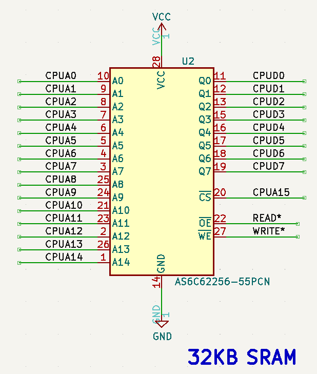
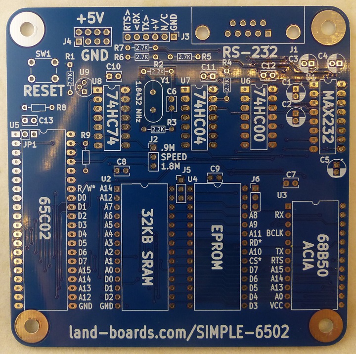
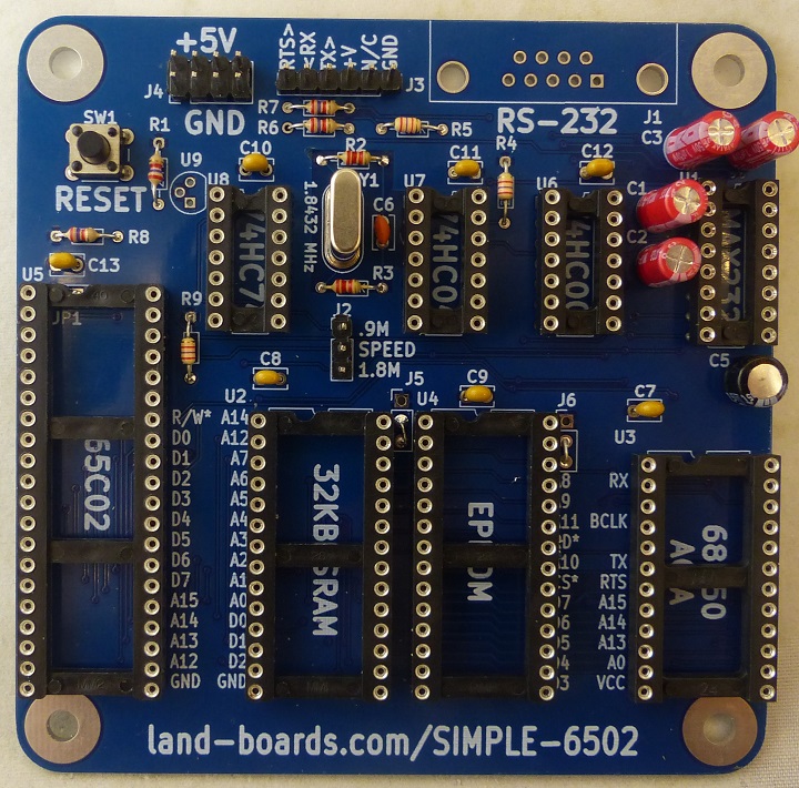
- 0x0000-0x7FFF 32KB SRAM
- 0x8000-0x9FFF Free Space (8KB)
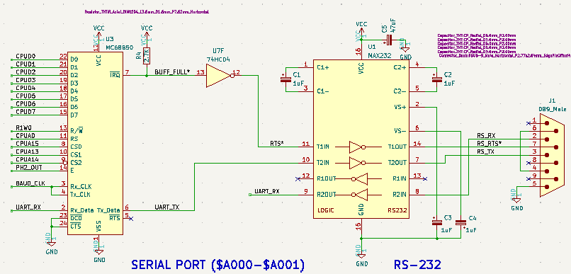
- 0xA000-0xBFFF Serial (ACIA)
- 0xC000-0xCFFF 16KB EPROM
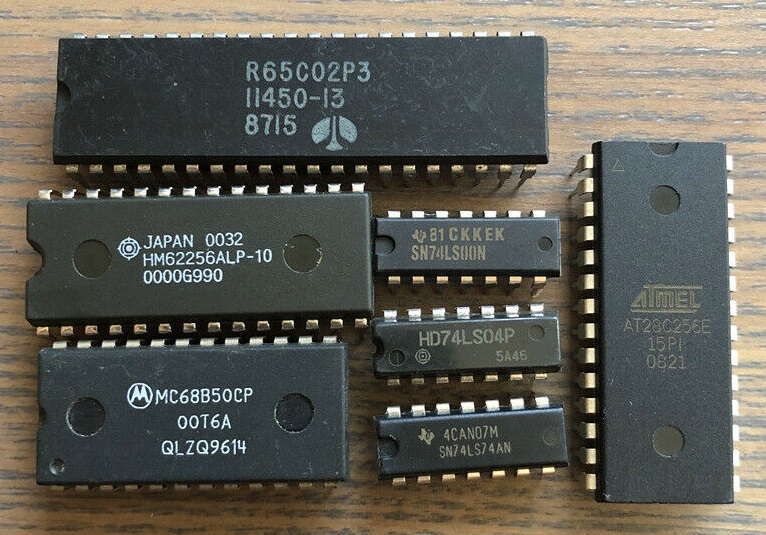
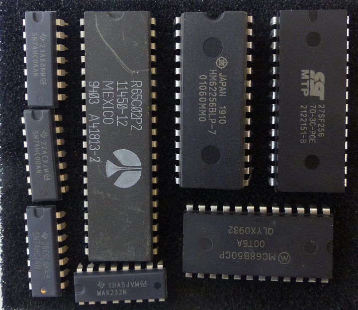
Chip Set


References
Design


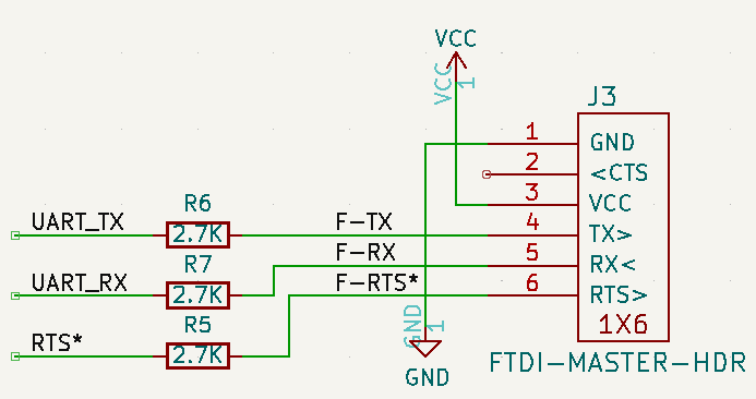
- FTDI
- Does not match Grant's pinout


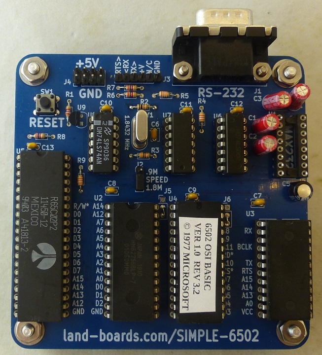
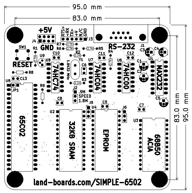
J1 - RS-232 Serial
- DB-9 Male
- Matches Grant's pinout
- Pinout
- N/C
- Receive
- Transmit
- Loop to pin 6
- GND
- Loop to pin 4
- RTS
- N/C
- N/C
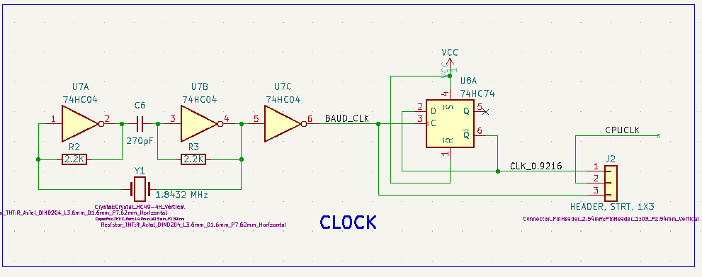
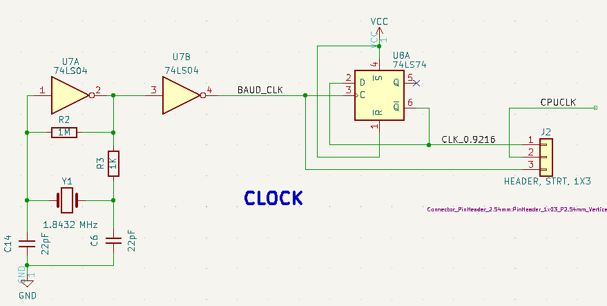
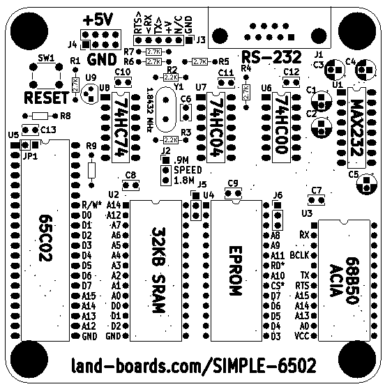
J2 - Speed Select Jumper
- 1-2 - 0.92 MHz
- 2-3 = 1.8432 MHz
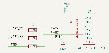
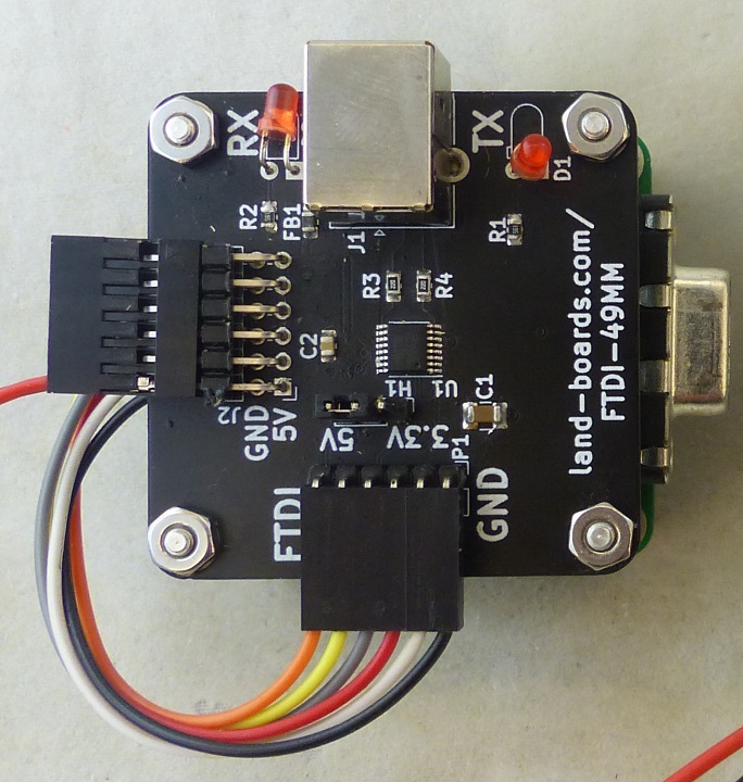
J3 - FTDI / TTL Serial
- Requires a FTDI cross-over cable

- GND
- RTS* (out)
- +5V
- Receive (in)
- Transmit (out)
- N/C
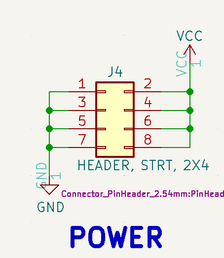
J4 - 5V Power

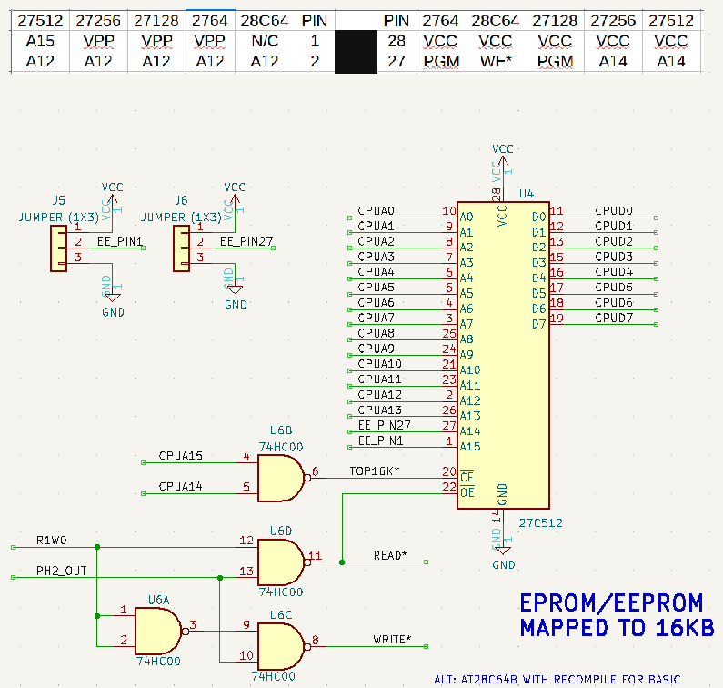
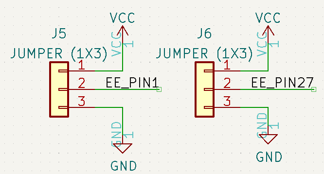
J5 / J6 - EPROM/EEPROM Select Jumpers

- J5 - EPROM Pin 1 jumper
- 1-2 for 28C64, 28C256 (Pull WE to VCC)
- 2-3 for 27256, 27SF256, 27512 (Pull A14 to GND)
- J6 - EPROM Pin 27 jumper
EEPROM Pin Table
| 27512
|
27256
|
27SF256
|
28C256
|
27128
|
2764
|
28C64
|
PIN
|
|
PIN
|
2764
|
28C64
|
27128
|
28C256
|
27SF256
|
27256
|
27512
|
| A15
|
VPP
|
VPP
|
A14
|
VPP
|
VPP
|
N/C
|
1
|
|
28
|
VCC
|
VCC
|
VCC
|
VCC
|
VCC
|
VCC
|
VCC
|
| A12
|
A12
|
A12
|
A12
|
A12
|
A12
|
A12
|
2
|
|
27
|
PGM
|
WE*
|
PGM
|
WE*
|
A14
|
A14
|
A14
|
| A7
|
A7
|
A7
|
A7
|
A7
|
A7
|
A7
|
3
|
|
26
|
A13
|
N/C
|
A13
|
A13
|
A13
|
A13
|
A13
|
| A6
|
A6
|
A6
|
A6
|
A6
|
A6
|
A6
|
4
|
|
25
|
A8
|
A8
|
A8
|
A8
|
A8
|
A8
|
A8
|
| A5
|
A5
|
A5
|
A5
|
A5
|
A5
|
A5
|
5
|
|
24
|
A9
|
A9
|
A9
|
A9
|
A9
|
A9
|
A9
|
| A4
|
A4
|
A4
|
A4
|
A4
|
A4
|
A4
|
6
|
|
23
|
A11
|
A11
|
A11
|
A11
|
A11
|
A11
|
A11
|
| A3
|
A3
|
A3
|
A3
|
A3
|
A3
|
A3
|
7
|
|
22
|
OE*
|
OE*
|
OE*
|
OE*
|
OE*
|
OE*
|
OE*
|
| A2
|
A2
|
A2
|
A2
|
A2
|
A2
|
A2
|
8
|
|
21
|
A10
|
A10
|
A10
|
A10
|
A10
|
A10
|
A10
|
| A1
|
A1
|
A1
|
A1
|
A1
|
A1
|
A1
|
9
|
|
20
|
CE*
|
CE*
|
CE*
|
CE*
|
CE*
|
CE*
|
CE*
|
| A0
|
A0
|
A0
|
A0
|
A0
|
A0
|
A0
|
10
|
|
19
|
D7
|
D7
|
D7
|
D7
|
D7
|
D7
|
D7
|
| D0
|
D0
|
D0
|
D0
|
D0
|
D0
|
D0
|
11
|
|
18
|
D6
|
D6
|
D6
|
D6
|
D6
|
D6
|
D6
|
| D1
|
D1
|
D1
|
D1
|
D1
|
D1
|
D1
|
12
|
|
17
|
D5
|
D5
|
D5
|
D5
|
D5
|
D5
|
D5
|
| D2
|
D2
|
D2
|
D2
|
D2
|
D2
|
D2
|
13
|
|
16
|
D4
|
D4
|
D4
|
D4
|
D4
|
D4
|
D4
|
| GND
|
GND
|
GND
|
GND
|
GND
|
GND
|
GND
|
14
|
|
15
|
D3
|
D3
|
D3
|
D3
|
D3
|
D3
|
D3
|
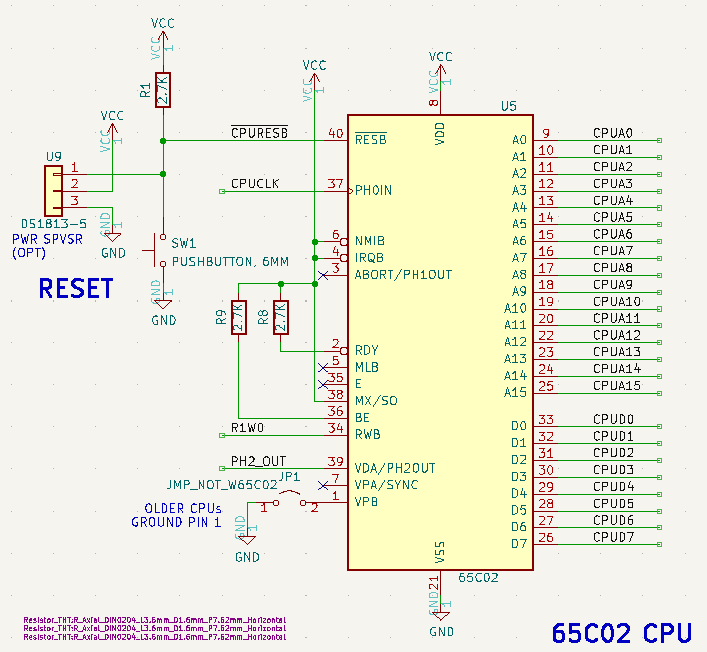
JP1 - CPU Pin 1
- Install if CPU is not a WDC 65C02 or WDC 65C816
Software
- Link to Grant's files
- Source code
- osi_bas.s <== the Microsoft OSI BASIC and I/O routines SOURCE all in a single file
- Grant's I/O routines are at the end of it
- Files to allow the source to be assembled on a Windows based machine
- assemble.bat <== double click to assemble osi_bas.s and link to binary file "osi_bas.bin"
- This should be exactly 16K
- osi_bas.cfg <== configuration file for the linker (ensure ORG and entries in this file match if you change any)
- ca65.exe <== the assembler from the cc65 package. Use this. The new version on the cc65 site crashes!
- ld65.exe <== linker from the cc65 package
- Output files
- osi_bas.bin <== the ROM fine in pure binary
- osi_bas.lst <== Assembly listing file
- rom.hex <== the ROM fine in standard INTEL-HEX format
- To allow simple re-assembly, extract all files to the same folder
- Freeware utilities are available to convert the "bin" file to HEX or s19 (etc) - use your internet search tool to find
- All source code, assembler binaries and the HEX dump of the ROM is here
- It is in standard INTEL-HEX format for uploading to a suitable programmer.
First Unit Checkout

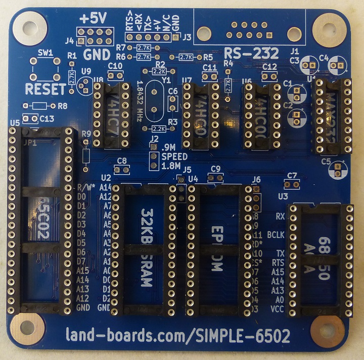
Install Sockets

Install Passives

Power
- Install 2x4 at J4
- Power card via J4 with 5V
- Check power pins on parts
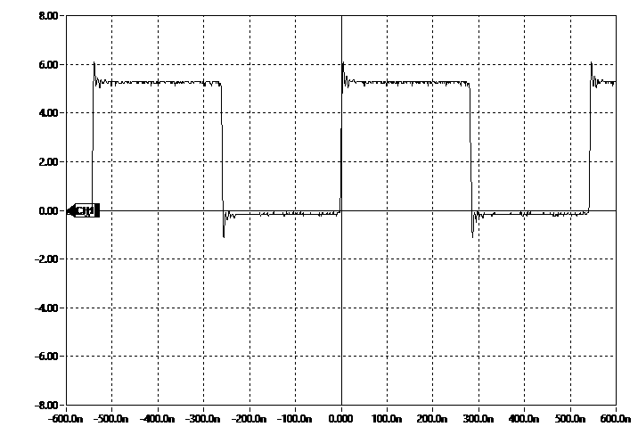
Clock
- Install Clock parts
- Did not have 270 pF cap, used 220 pF
- U7 (74HC04)
- Y1 1.8432 MHz crystal
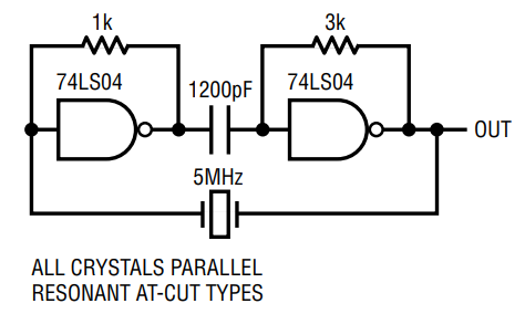
- Clock "doubling" with 74HC04 part
- Worse with 74HC14
- Switched to 74LS04 - works well
- Install clock divider
- Check clocks at J2
- Pin 1 s/b 0.9216 MHz
- Pin 3 s/b 1.8432 MHz
- Outputs are OK
- Need to change P/L and S/S to 74LS04


- Used 1nF cap instead of 1200pF
- Starts reliably but has a glitch
- Seems to run OK
- Reset is weird, sometimes does not boot and takes a couple of presses
- Not sure if this is clock related
- Order new 74LS04 parts
- See Rev 2 updates
Reset
- Install U9
- Install pushbutton switch SW1
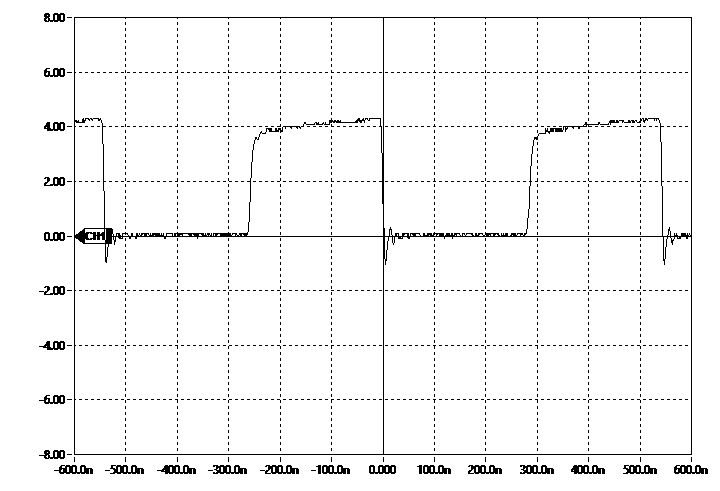
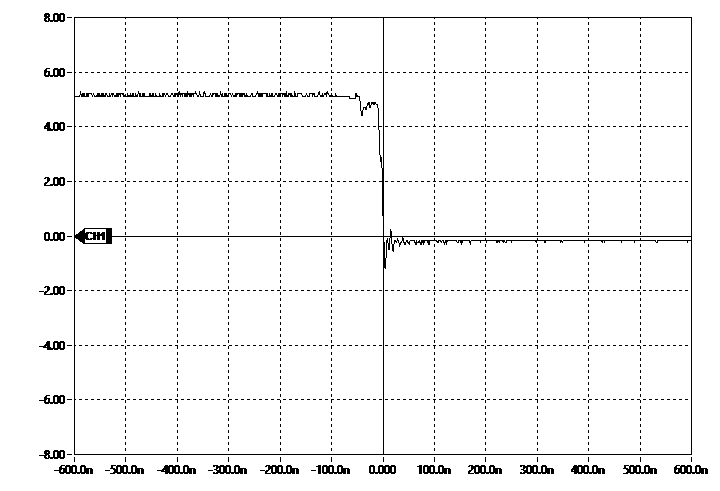
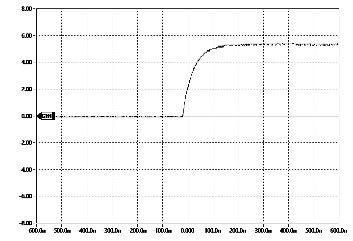
- Reset button gets stretched by Power Monitor U9
- Measure at 6502 U5 pin 40
- Falling edge scope cap


- Switch failed, replaced - works
EPROM
- SST27C256 EEPROM
- 32 KB part
- Using first 16KB of EEPROM
- J5 EEPROM pin 1 = VPP = VCC or GND
- J6 EEPROM pin 27 = A14 = GND
- U1 - Do not install MAX232
- R65C02 CPU
- Install JP1 on rear of card as wire
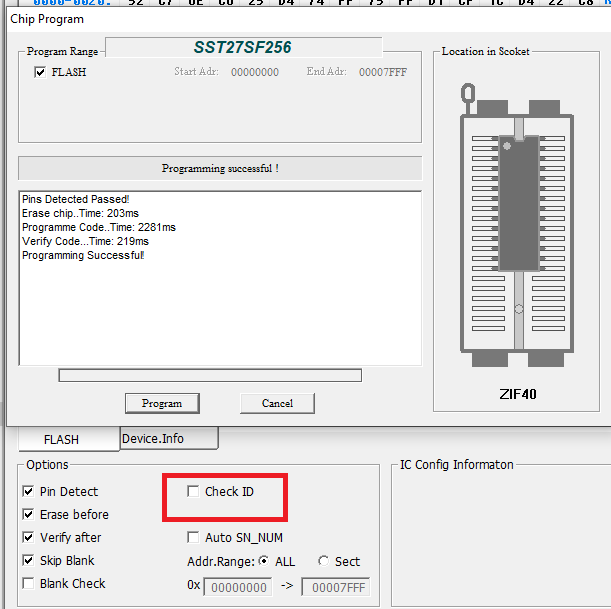
EEPROM Programming

- Device programmed/verified
Install CPU, ROM, RAM, ACIA
- Do not install MAX232 yet
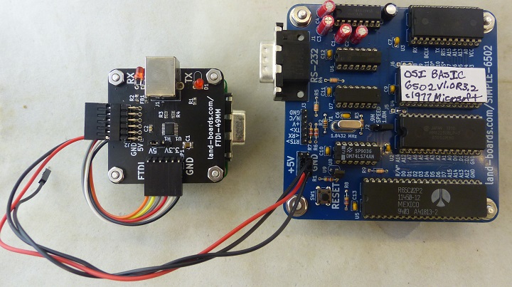
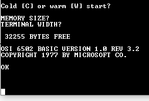
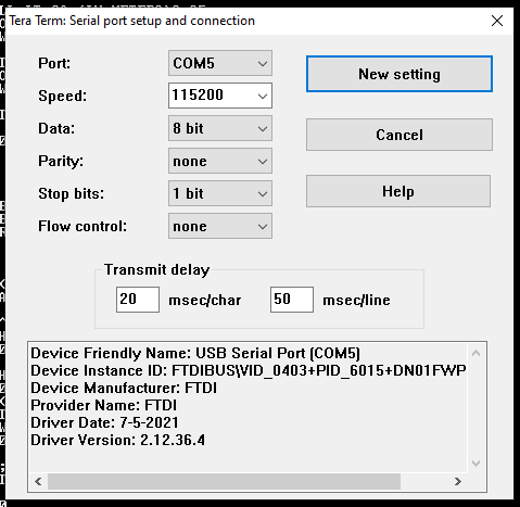
Test FTDI Serial
Card Without MAX232
- With DB-9 connector
- Install DB-9 Male
- Holes don't line up well, but 4-40 screws can fit
- Without MAX232

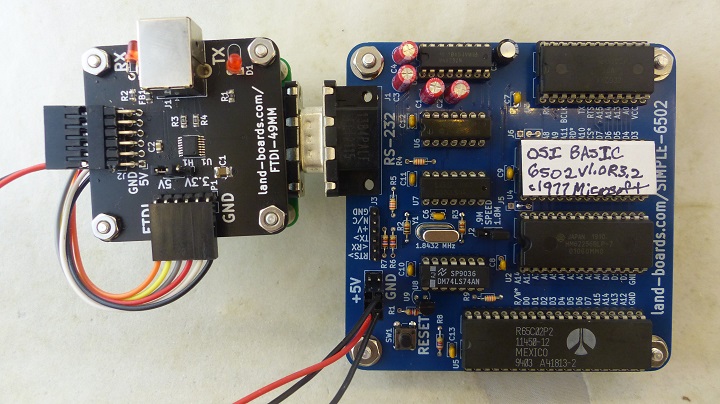
Built Card


- DB-9 connectors connected together


Performance

10 FOR I =1 TO 10000
20 PRINT I
30 NEXT I
Mechanicals

PCB Issues
Rev 2
- See clock section above for changes

- R8, R9 missing 2.7K silkscreen
- C6, C14 change to 33 pF
- Symptom with 22 pF caps was wrong oscillation frequency
- Crystal is 18pF
- Matching caps should be 2x (since the caps are essentially in series
- 36pF would be right, but there's also pin and PCB capacitance so use 33 pF caps
- U7 has to be 74HC04 with these other value parts
- Measured oscillator circuit timing/voltages

Rev 1
Assembly Sheet
Assembly Sheet Rev 2
Assembly Sheet Rev 1
