Features
- 65C02 or 65C816 CPU
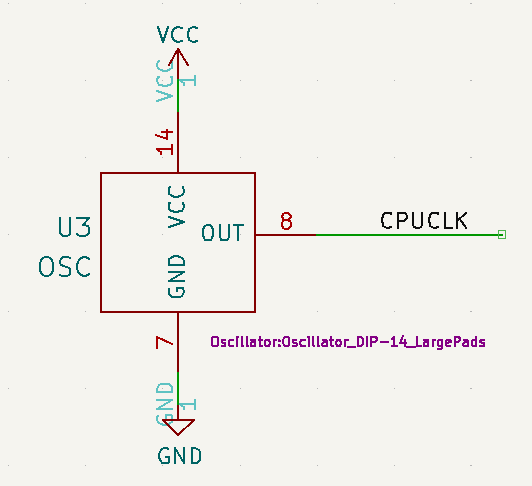
- 2 MHz (typical) Oscillator on card
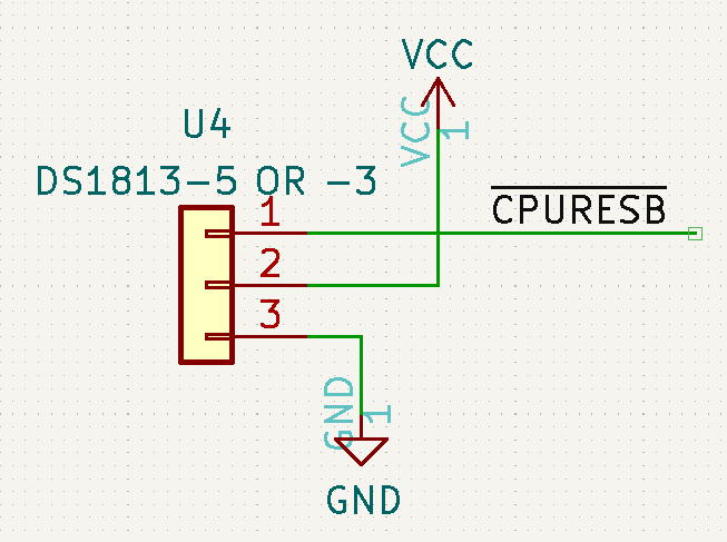
- Reset switch/power monitor
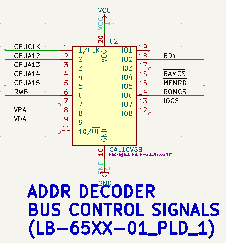
- Address decoder PLD drives RAM/ROM/IO chip selects
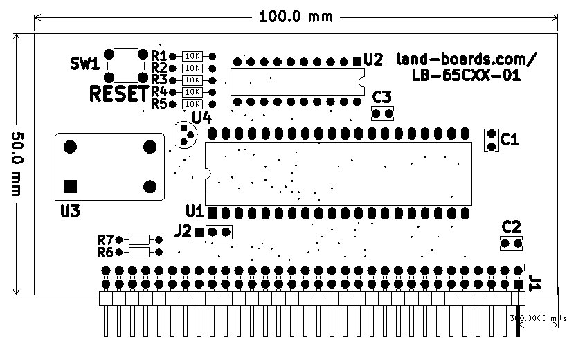
- 100x50mm card
Design
Memory Map
0x0000-0x7FFF - 32KB SRAM
0x8000-0x8FFF - 4KB I/O space
0x9000-0xBFFF - Free space (12 KB SRAM Using 128KB SRAM)
0xC000-0xFFFF - 16KB EPROM space
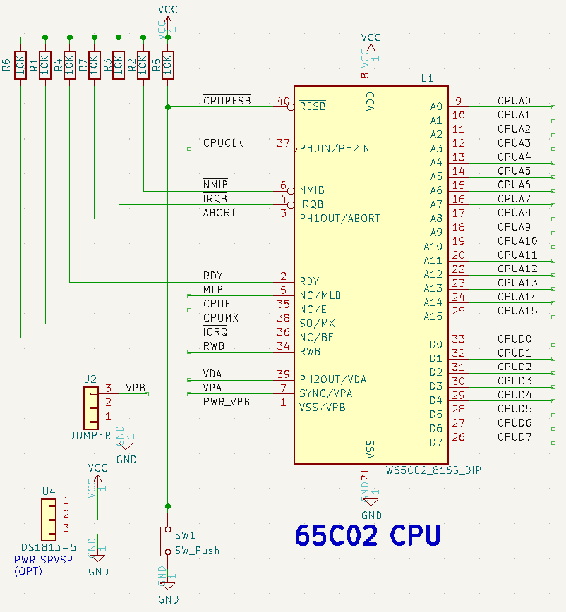
CPU

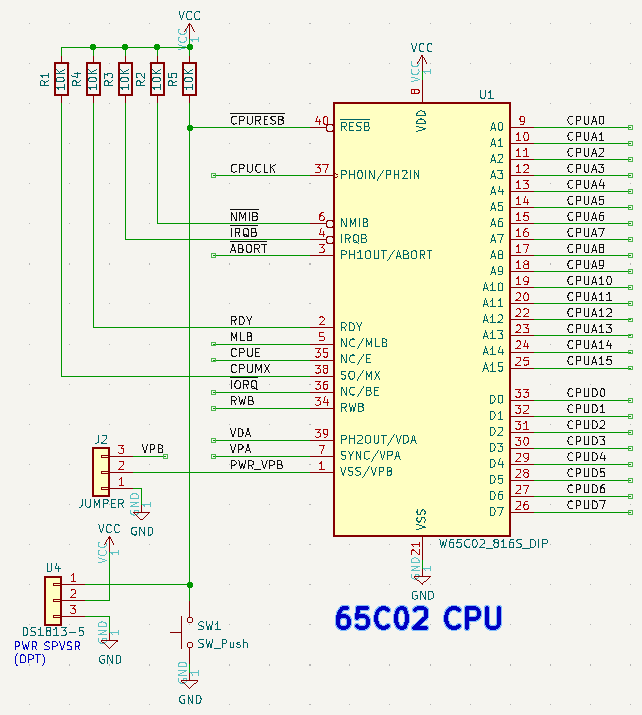
- 65C02 or 65C816 CPU
- 65C816 requires mods to the PCB (see Checkout notes below) or Rev 2 PCB
- 2 MHz
- Install jumper J2:1-2 if CPU is not a WDC 65C02 or WDC 65C816
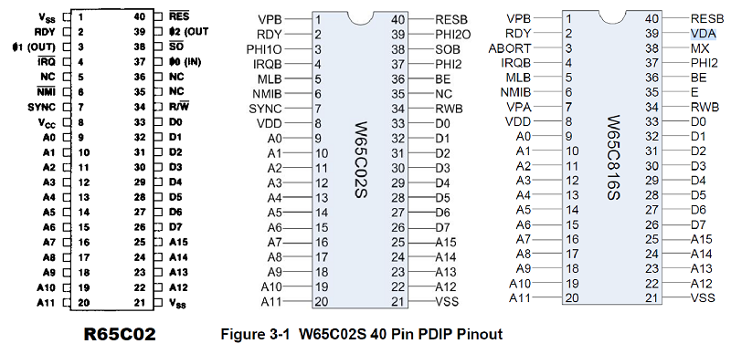
R65C02 vs W65C02 vs W65C816 CPUs
| U1 Pin
|
U1 Pin Name
|
Sig Name
|
Pullup
|
R65C02 sig
|
W65C02 sig
|
W65C816 sig
|
| 1
|
VSS/VPB
|
J2 selects
|
N
|
VSS (IN)
|
VPB (OUT)
|
VPB (OUT)
|
| 3
|
PH1OUT/ABORT
|
ABORT*
|
REV2
|
PH1OUT (OUT)
|
PH1OUT (OUT)
|
ABORT (IN)
|
| 5
|
NC/MLB
|
MLB
|
N
|
NC
|
MLB (OUT)
|
MLB (OUT)
|
| 7
|
SYNC/VPA
|
VPA
|
N
|
SYNC (OUT)
|
SYNC (OUT)
|
VPA (OUT)
|
| 35
|
NC/E
|
CPUE
|
N
|
NC
|
NC
|
EM/NAT (OUT)
|
| 36
|
NC/BE
|
IORQ*
|
REV2
|
NC
|
BE (IN)
|
BE (IN)
|
| 37
|
PH0IN/PH2IN
|
CPUCLK
|
N
|
PH0IN
|
PH2IN
|
PH2IN
|
| 38
|
SO/MX
|
CPUMX
|
REV1/2
|
SO* (IN)
|
SOB (IN)
|
MX (OUT)
|
| 39
|
PH2OUT/VDA
|
VDA
|
N
|
PH2OUT (OUT)
|
PH2OUT (OUT)
|
VDA (OUT)
|

VDA/VPA (65C816)
- VDA/VDA
- 00, Internal operation (invalid address bus)
- 01, Valid Program Address
- 10, Valid Data Address
- 11, Opcode-fetch
Chip Set

- Picture shows 3 MHz CPU
- Received 2 MHz CPU
- As received:

Oscillator

PLD

PLD Listing
Name       LB-65CXX-01_PLD;
Partno     ATF16V8B;
Date       09/12/24;
Revision   01;
Designer   DOUG G;
Company    LAND BOARDS LLC;
Assembly   LB65CXX01_U2;
Location   Rustbelt, US;
Device     G16V8;

/*
	65C02 Control
*/

/* Control inputs */
PIN    1   = CLK;
PIN    2   = CPUA12;
PIN    3   = CPUA13;
PIN    4   = CPUA14;
PIN    5   = CPUA15;
PIN    6   = CPUREAD;
PIN    8   = VPA;
PIN    9   = VDA;		/* Pin 39, PH2OUT - Enable line */

/* Address Decode and Chip Select outputs */
PIN    13  = !IOCS;
PIN    14  = !ROMCS;
PIN    15  = !MEMRD;
PIN    16  = !RAMCS;
PIN    18  = RDY;

RAMCS = !CPUA15 & CPUREAD		/* 0x0000-0x7FFF */
#       !CPUA15 & !CPUREAD & VDA;

IOCS = CPUA15 & !CPUA14 & CPUA13 & !CPUA12 & CPUREAD	/* 0x8000-0x8FFF */
#      CPUA15 & !CPUA14 & CPUA13 & !CPUA12 & !CPUREAD & VDA;

ROMCS = CPUA15 & CPUA14 & CPUREAD;	/* 0xC000-0xFFFF (16KB space)		*/

RDY = VDA;

MEMRD = CPUREAD;
Reset Controller

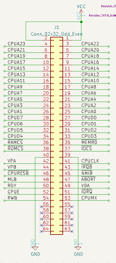
Backplane connector

Software
Assembly Language Development Toolchain
ca65 AciaTest.s -o AciaTest.o -l
ld65 -C AciaTest.cfg AciaTest.o -o AciaTest.bin
srec_cat.exe AciaTest.bin -binary -o AciaTest.hex -Intel
MEMORY {
	ROM:		start = $C000, size = $3FFA, fill = yes, fillval=$FF, file = %O;
	VECTS:		start = $FFFA, size = $6, fill = yes, fillval=$FF, file = %O;
}

SEGMENTS {
	CODE:		load = ROM,	type = ro;
	VECTS:		load = VECTS,	type = ro;
}
ACIA Test Code
Simple Monitor 6502
- SimpleMon6502.s - GitHub repo
- Contains
- ACIA init, read, write
- Simplest commands mostly for function development
- String functions
- Read a string
- Write a string (macro)
- Write hex value as a string
- Dump page (256-bytes) of memory
6502 Enhanced BASIC
?FRE(0)
 31999
Enhanced BASIC Bug Fixes
; Ibuffs can now be anywhere in RAM, ensure that the max length is < $80,
; the input buffer must not cross a page boundary and must not overlap with
; program RAM pages!

;Ibuffs            = IRQ_vec+$14
Ibuffs            = VEC_SV+$16
                              ; start of input buffer after IRQ/NMI code
Ibuffe            = Ibuffs+$47; end of input buffer
- Boots to request memory size


OSI BASIC
- LB-6502 GitHub
- Create your own Version of Microsoft BASIC for 6502
- Grant Searle's 6502 design
- Source code
- osi_bas.s <== the Microsoft OSI BASIC and I/O routines SOURCE all in a single file
- Grant's I/O routines are at the end of it
- Files to allow the source to be assembled on a Windows based machine
- assemble.bat <== double click to assemble osi_bas.s and link to binary file "osi_bas.bin"
- This should be exactly 16K
- osi_bas.cfg <== configuration file for the linker (ensure ORG and entries in this file match if you change any)
- ca65.exe <== the assembler from the cc65 package. Use this. The new version on the cc65 site crashes!
- ld65.exe <== linker from the cc65 package
- srec_cat.exe <== Converts bin file to .hex file
- Output files
- osi_bas.bin <== the ROM fine in pure binary
- osi_bas.lst <== Assembly listing file
- rom.hex <== the ROM fine in standard INTEL-HEX format
- To allow simple re-assembly, extract all files to the same folder
- Use srec_cat utility to convert the "bin" file to HEX or s19 (etc)
- All source code, assembler binaries and the HEX dump of the ROM is here
- It is in standard INTEL-HEX format for uploading to a suitable programmer.
- Having trouble running code
Programming References
6502 Instruction Set
Additional Tools
Mechanicals

Checkout
Rev 3
PCB Updates
- Add bulk electrolytic cap
- Make PH2OUT on VPB backplane line (swap wth VDA)
- Change to vertical reset switch
- Add an LED that is written by writing D0 to ROM area
Rev 2
Rev 2 Checkout
- Install jumper J2:1-2 since CPU is R65C02
- NOP tester - 6502 nop = 0xEA
- Add LED
- 1.8K resistor from U2-17 to Ground
- Wire U2-11 to U1-33 CPUD0

- Cut etch U1-39 in rear (removes PH2OUT from backplane)

- Add wire U1-39 to J2-3 (PH2OUT/VPB on VPB output)

Rev 2 Changes
- Add pull-up resistor on ABORT* line (U1-3)
- Add pull-up resistor on BE line (U1-36)

Rev 1
- Install jumper J2:1-2 if CPU is not a WDC 65C02 or WDC 65C816
- If WDC 65C02 or WDC 65C816 is used:
- Add pull-up resistor on ABORT* line (U1-3)
- Add pull-up resistor on BE line (U1-36)
Assembly Sheet
Rev 2
Rev 1

