Work in Progress

Build
FPGA
Software
Disk Images
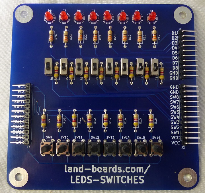
Configuration Switches/Jumpers/LEDs
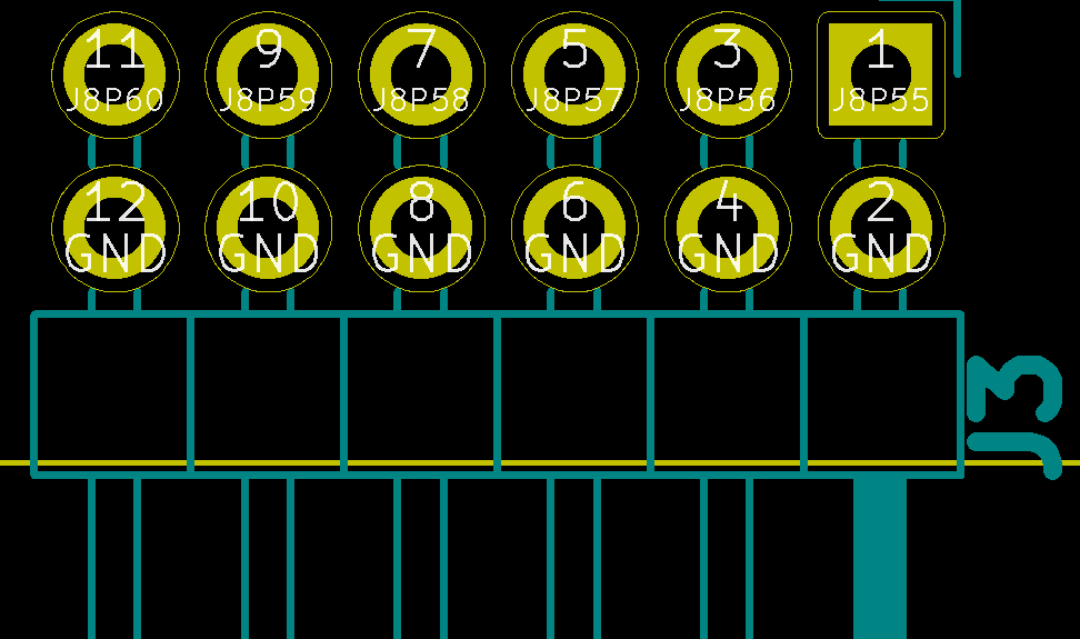
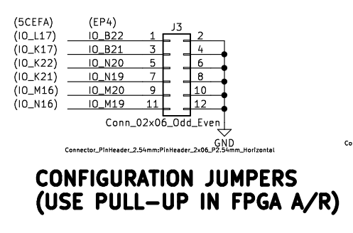
J3 - Configuration Jumpers (5CEFA2F23 FPGA Card pin numbers)


| DRIVE
|
VALUE
|
SW3
|
SW2
|
SW1
|
| rl
|
SELECT
|
OUT
|
OUT
|
IN
|
| rk
|
SELECT
|
OUT
|
IN
|
OUT
|
| rp
|
SELECT
|
IN
|
OUT
|
OUT
|
|
|
J3
|
5, 6
|
3,4
|
1,2
|
|
|
FPGA PIN
|
PIN_K22
|
PIN_K17
|
PIN_L17
|
Switches

| Function
|
J10 Pin
|
FPGA Pin
|
| resetbtn
|
SW9
|
PIN_J16
|
Connectors
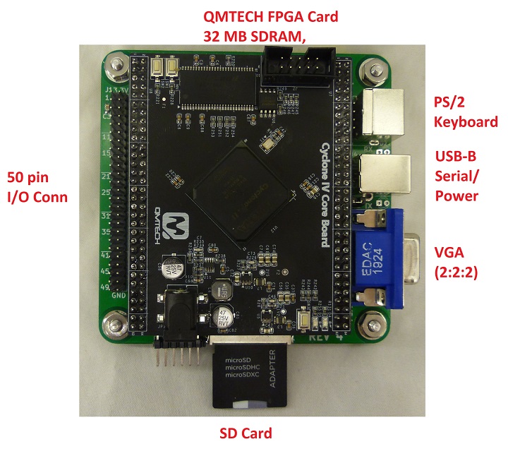
P1 - VGA (5CEFA2F23 Card)
- videoR0 = U8-49 = PIN_E12
- videoR1 = U8-50 = PIN_D12
- videoG0 = U8-51 = PIN_D13
- videoG1 = U8-52 = PIN_C13
- videoB0 = U8-53 = PIN_B13
- videoB1 = U8-54 = PIN_A13
- hSync = U8-55 = PIN_A15
- vSync = U8-56 = PIN_A14
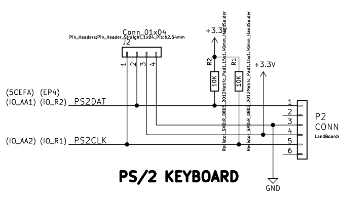
P2 - PS/2 Keyboard

- PS2DAT = U7-8 = PIN_BANK_2A_AA1
- PS2CLK = U7-8 = PIN_NANK_2A_AA2
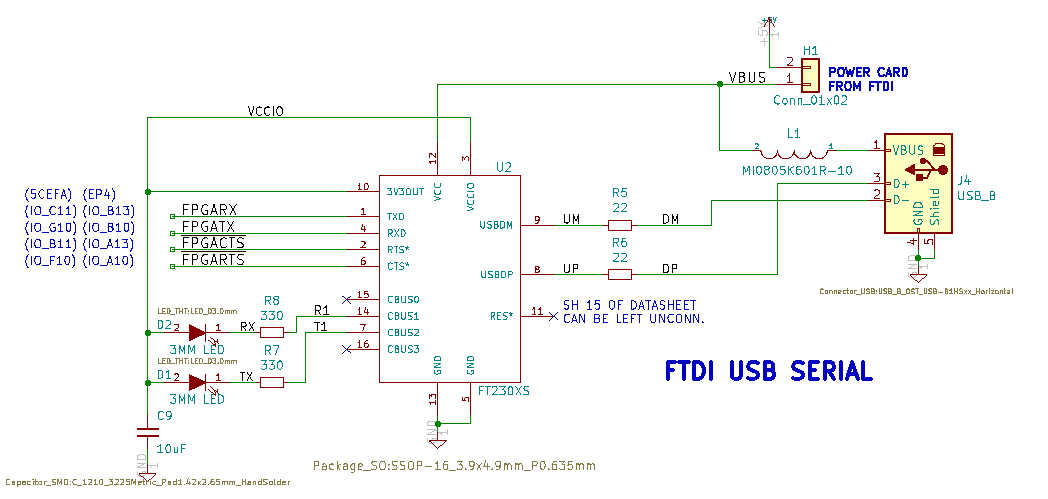
P3 - Serial Ports - I/O connector
- fpgaRx1 (in) = PIN_C11
- Needs weak pullup
- set_instance_assignment -name WEAK_PULL_UP_RESISTOR ON -to rxd1
- fpgaTx1 (out) = PIN_G10
- fpgaRts1 = U7-44 = PIN_F10
- fpgaCts1 = U7-46 = PIN_B11
IO conn
- Second serial port on I/O connector
- rx2 (in) = PIN_M18
- tx2 (out) = PIN_L19
- rts2 (out) = PIN_N19
- cts2 (in) = PIN_M21
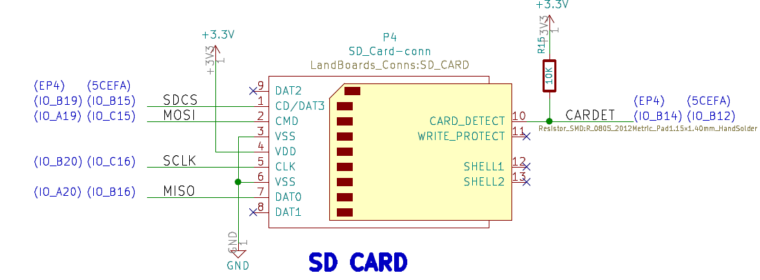
P4 - SD Card (5CEFA2F23 FPGA pin numbers)
- This build only works with SD Cards, not SD/HC or other newer cards.
- These cards are 1 GB or 2 GB in size.

- SDCS = U7-57 = PIN_BANK_7A_B15
- MOSI = U7-58 = PIN_BANK_7A_C15
- SCK = U7-59 = PIN_BANK_7A_C16
- MISO = U7-60 = PIN_BANK_7A_B16
- SD_DETECT - PIN_B12
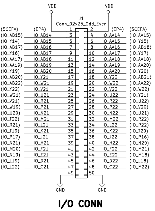
J1 - I/O Connector (5CEFA2F23 FPGA Card pin numbers)

- J1-50 = GND
- J1-49 = GND
- J1-48 = PIN_M22 = resetbtn
- J1-47 = PIN_L22 = n/a
- J1-46 = PIN_L18 = tx1
- J1-45 = PIN_L19 = rx1
- J1-44 = PIN_M18 = rts1
- J1-43 = PIN_N19 = cts1
- J1-42 = PIN_M21 = n/a
- J1-41 = PIN_M20 = n/a
- J1-40 = PIN_N20 = xu_sclk
- J1-39 = PIN_N21 = xu_mosi
- J1-38 = PIN_P16 = xu_miso
- J1-37 = PIN_P17 = xu_debug_tx
- J1-36 = PIN_T20 = xu_cs
- J1-34 = PIN_P22 = greenled[1]
- J1-33 = PIN_R21 = greenled[0]
- J1-32 = PIN_R22 = greenled[3]
- J1-31 = PIN_T22 = greenled[2]
- J1-29 = PIN_U20 = greenled[4]
- J1-1 = VCC
- J1-2 = VCC
J4 - USB-B B (5CEFA2F23 FPGA Card pin numbers) Serial Port
- On-board FT230X FTDI USB to Serial

Resources
Programming the FPGA EEPROM (5CEFA2F23 FPGA)
- File
- Convert Programming File
- Configuration Device = MT25QL128
- Mode = Active Serial
- Programming File Type: *.jic
- Advanced = Check both Disables...
- Select Flash Loader
- Add Device = Cyclone V and 5CEFA2
- Select SOF Data
- Select Add File and select the .sof file
- Generate
- In Tools, Programmer
- Mode: JTAG
- Add file and select the .jic file
- Select Program/Configure
- Takes a while to program
- Press button near VGA
Pin List
# Analysis & Synthesis Assignments
# ================================
set_global_assignment -name FAMILY "Cyclone V"
set_global_assignment -name TOP_LEVEL_ENTITY top
set_global_assignment -name EDA_DESIGN_ENTRY_SYNTHESIS_TOOL "Design Compiler"

# Fitter Assignments
# ==================
set_global_assignment -name DEVICE 5CEFA2F23I7
set_global_assignment -name STRATIX_DEVICE_IO_STANDARD "3.3-V LVTTL"
set_global_assignment -name CRC_ERROR_OPEN_DRAIN OFF
set_global_assignment -name CYCLONEII_RESERVE_NCEO_AFTER_CONFIGURATION "USE AS REGULAR IO"
set_global_assignment -name FORCE_CONFIGURATION_VCCIO ON

# Pin & Location Assignments
# ==========================

# Clock and external reset button
set_location_assignment PIN_M9 -to clkin
set_location_assignment PIN_M22 -to resetbtn
set_instance_assignment -name WEAK_PULL_UP_RESISTOR ON -to resetbtn
# Control switches
set_location_assignment PIN_L22 -to sw_cont
set_instance_assignment -name WEAK_PULL_UP_RESISTOR ON -to sw_cont
set_location_assignment PIN_L18 -to sw_halt
set_instance_assignment -name WEAK_PULL_UP_RESISTOR ON -to sw_halt
set_location_assignment PIN_M20 -to led_run
# Jumpers on front edge
set_location_assignment PIN_L17 -to switch[0]
set_location_assignment PIN_K17 -to switch[1]
set_location_assignment PIN_K22 -to switch[2]
set_location_assignment PIN_K21 -to switch[3]
# SDRAM
set_location_assignment PIN_Y9 -to dram_addr[12]
set_location_assignment PIN_T9 -to dram_addr[11]
set_location_assignment PIN_R6 -to dram_addr[10]
set_location_assignment PIN_W8 -to dram_addr[9]
set_location_assignment PIN_T8 -to dram_addr[8]
set_location_assignment PIN_U8 -to dram_addr[7]
set_location_assignment PIN_V6 -to dram_addr[6]
set_location_assignment PIN_U7 -to dram_addr[5]
set_location_assignment PIN_U6 -to dram_addr[4]
set_location_assignment PIN_N6 -to dram_addr[3]
set_location_assignment PIN_N8 -to dram_addr[2]
set_location_assignment PIN_P7 -to dram_addr[1]
set_location_assignment PIN_P8 -to dram_addr[0]
set_location_assignment PIN_P9 -to dram_ba_1
set_location_assignment PIN_T7 -to dram_ba_0
set_location_assignment PIN_AA7 -to dram_cas_n
set_location_assignment PIN_V9 -to dram_cke
set_location_assignment PIN_AB11 -to dram_clk
set_location_assignment PIN_AB5 -to dram_cs_n
set_location_assignment PIN_P12 -to dram_dq[15]
set_location_assignment PIN_R12 -to dram_dq[14]
set_location_assignment PIN_U12 -to dram_dq[13]
set_location_assignment PIN_R11 -to dram_dq[12]
set_location_assignment PIN_R10 -to dram_dq[11]
set_location_assignment PIN_U11 -to dram_dq[10]
set_location_assignment PIN_T10 -to dram_dq[9]
set_location_assignment PIN_U10 -to dram_dq[8]
set_location_assignment PIN_AA8 -to dram_dq[7]
set_location_assignment PIN_AB8 -to dram_dq[6]
set_location_assignment PIN_AA9 -to dram_dq[5]
set_location_assignment PIN_Y10 -to dram_dq[4]
set_location_assignment PIN_AB10 -to dram_dq[3]
set_location_assignment PIN_AA10 -to dram_dq[2]
set_location_assignment PIN_Y11 -to dram_dq[1]
set_location_assignment PIN_AA12 -to dram_dq[0]
set_location_assignment PIN_V10 -to dram_udqm
set_location_assignment PIN_AB7 -to dram_ldqm
set_location_assignment PIN_AB6 -to dram_ras_n
set_location_assignment PIN_W9 -to dram_we_n
# Serial port (USB-to-Serial)
set_location_assignment PIN_C11 -to rx1
set_location_assignment PIN_G10 -to tx1
set_location_assignment PIN_F10 -to rts1
set_location_assignment PIN_B11 -to cts1
# Second serial port
set_location_assignment PIN_L19 -to tx2
set_location_assignment PIN_M18 -to rx2
set_location_assignment PIN_M21 -to cts2
set_location_assignment PIN_N19 -to rts2
# SD Card
set_location_assignment PIN_C16 -to sdcard_sclk
set_location_assignment PIN_B15 -to sdcard_cs
set_location_assignment PIN_B16 -to sdcard_miso
set_location_assignment PIN_C15 -to sdcard_mosi
# Seven segment display (on J1)
set_location_assignment PIN_R21 -to max7219_clock
set_location_assignment PIN_P22 -to max7219_data
set_location_assignment PIN_T19 -to max7219_load
# Ethernet
set_location_assignment PIN_T20 -to xu_cs
set_location_assignment PIN_P17 -to xu_debug_tx
set_location_assignment PIN_P16 -to xu_miso
set_location_assignment PIN_N21 -to xu_mosi
set_location_assignment PIN_N20 -to xu_sclk
# PS/2 Keyboard
set_location_assignment PIN_AA2 -to ps2k_c
set_location_assignment PIN_AA1 -to ps2k_d
# Video
set_location_assignment PIN_A15 -to vgah
set_location_assignment PIN_A14 -to vgav
set_location_assignment PIN_A13 -to o_vgab[1]
set_location_assignment PIN_B13 -to o_vgab[0]
set_location_assignment PIN_C13 -to o_vgag[1]
set_location_assignment PIN_D13 -to o_vgag[0]
set_location_assignment PIN_D12 -to o_vgar[1]
set_location_assignment PIN_E12 -to o_vgar[0]
