Difference between revisions of "Colpitts XTAL Oscillator Rev 1 Assembly Sheet"
Jump to navigation
Jump to search
Blwikiadmin (talk | contribs) (Created page with "== PL == {| class="wikitable" ! Qty ! Value ! RefDes ! ! Qty ! Value ! RefDes |- | 1 | 0.1uF | C4 | | 1 | Conn_01x06 | J2 |- | 1 | 100pF | C3 | | 1 | DCJ0202 | J3 |- | 2 |...") |
Blwikiadmin (talk | contribs) (→PL) |
||
| (5 intermediate revisions by the same user not shown) | |||
| Line 1: | Line 1: | ||
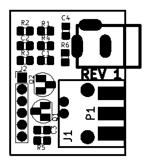
| + | [[file:Colpitts_XTAL_Osc-CAD.PNG]] | ||
| + | |||
== PL == | == PL == | ||
| Line 11: | Line 13: | ||
|- | |- | ||
| 1 | | 1 | ||
| − | | 0.1uF | + | | 0.1uF (0805) |
| C4 | | C4 | ||
| | | | ||
| 1 | | 1 | ||
| − | | | + | | Header, 1x6 |
| J2 | | J2 | ||
|- | |- | ||
| 1 | | 1 | ||
| − | | | + | | 10nF (0805) |
| C3 | | C3 | ||
| | | | ||
| 1 | | 1 | ||
| − | | | + | | DC Jack |
| J3 | | J3 | ||
|- | |- | ||
| 2 | | 2 | ||
| − | | | + | | 470pF (0805) |
| C1,C2 | | C1,C2 | ||
| | | | ||
| 1 | | 1 | ||
| − | | SMA | + | | SMA (opt) |
| P1 | | P1 | ||
| − | |||
| − | |||
| − | |||
| − | |||
| − | |||
| − | |||
| − | |||
| − | |||
|- | |- | ||
| 2 | | 2 | ||
| Line 47: | Line 41: | ||
| | | | ||
| 1 | | 1 | ||
| − | | | + | | BNC (opt) |
| − | | | + | | J1 |
|- | |- | ||
| 2 | | 2 | ||
| − | | 10K | + | | 10K (0805) |
| R1,R2 | | R1,R2 | ||
| | | | ||
| Line 59: | Line 53: | ||
|- | |- | ||
| 3 | | 3 | ||
| − | | 1K | + | | 1K (0805) |
| − | | R3 | + | | R3-R5 |
| − | |||
| − | |||
| − | |||
| | | | ||
| + | | 1 | ||
| + | | UUT | ||
| + | | Y1 | ||
|- | |- | ||
| 1 | | 1 | ||
| − | | 47 | + | | 47 (0805) |
| R6 | | R6 | ||
| | | | ||
| Line 75: | Line 69: | ||
|- | |- | ||
|} | |} | ||
| + | |||
| + | == Rework == | ||
| + | |||
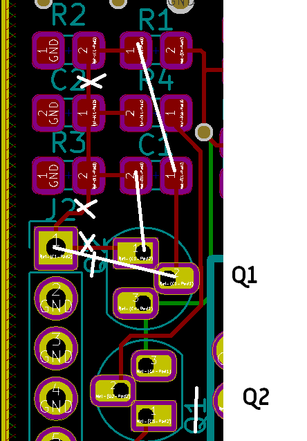
| + | [[file:Rework-rev1_Marks.png]] | ||
| + | |||
| + | * Cut etch R2 to C2 | ||
| + | * Cut etch R3 t J2-1 | ||
| + | * Cut etch J2-1 to (marked Q2) Emitter pin | ||
| + | * Add wire front side of PCB from R1 (to R2 side) to C1 (towards BNC side | ||
| + | * Add wire rear side of PCB from J2-1 to (marked Q2) Base pin | ||
| + | * Add wire front side of PCB C1 (to R3 side) to (marked Q2) Emitter pin | ||
Latest revision as of 22:37, 18 September 2021
PL
| Qty | Value | RefDes | Qty | Value | RefDes | |
|---|---|---|---|---|---|---|
| 1 | 0.1uF (0805) | C4 | 1 | Header, 1x6 | J2 | |
| 1 | 10nF (0805) | C3 | 1 | DC Jack | J3 | |
| 2 | 470pF (0805) | C1,C2 | 1 | SMA (opt) | P1 | |
| 2 | 2N3904 | Q1,Q2 | 1 | BNC (opt) | J1 | |
| 2 | 10K (0805) | R1,R2 | ||||
| 3 | 1K (0805) | R3-R5 | 1 | UUT | Y1 | |
| 1 | 47 (0805) | R6 |
Rework
- Cut etch R2 to C2
- Cut etch R3 t J2-1
- Cut etch J2-1 to (marked Q2) Emitter pin
- Add wire front side of PCB from R1 (to R2 side) to C1 (towards BNC side
- Add wire rear side of PCB from J2-1 to (marked Q2) Base pin
- Add wire front side of PCB C1 (to R3 side) to (marked Q2) Emitter pin

