GVSDuino
Contents
Features
We love the Arduino but have always found several aspects of deploying Arduinos into real-world applications to be particularly troubling. Our frustrations center around:
- Lack of decent mounting holes
- Limited number of power and ground pins
- Size of the card
- Jumper wires don't hold in female sockets very well
Not long into our time with the Arduino we discovered Sensor Shields. They solve the limitation for power and ground pins by providing a matching power and ground pin for every signal line. They also have male pins which tend to hold female cable pins better.
Sensor shields don't solve the size issue. In fact, they make the volume larger than it needs to be. They also don't change the fact that the mounting holes on the Arduino are difficult to use. The pins are either too close to connectors or power and we are always afraid of shorting them out in metal cases.
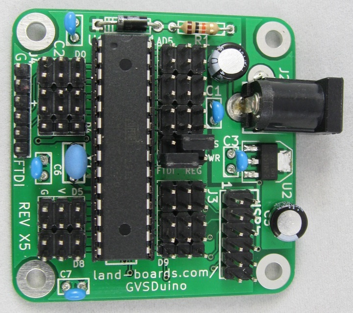
What makes it special? GVSDuino is the combination of an Arduino UNO and a GVS Shield. GVSDuino takes two awesome boards and puts them together on one board taking the best of each and improving on both. GVSDuino solved the two remaining issues we've always had with the Arduino. It has great mounting holes and it's smaller.
GVSDuino is a minimalist Arduino design without a USB interface so it requires an FTDI board such as the USB-to-TTL Converter board to connect up to a Host Computer. For many embedded applications that is not an issue.
GVSDuino has GVS connectors for all of the Processor I/O pins.
Headers/Connectors
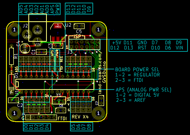
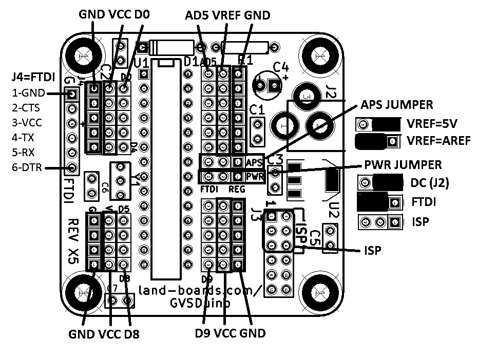
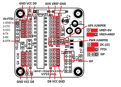
Digital D0-D13 GVS Headers
The Digital GVS D0-D13 headers surround the Microprocessor. The square pins are pin 1. The Microprocessor I/O connections on the headers are:
Pin	Function
1	GND
2	VCC
3	Signal
Analog AD0-AD5 GVS Headers
The Analog GVS AD0-AD5 headers surround the Microprocessor. The square pins are pin 1. The Microprocessor I/O connections on the headers are:
Pin	Function
1	GND
2	APS Jumper selection
3	Signal
- I2C
- A4 (SDA)
- A5 (SCL)
J2 - DC Power Connector
2.1mm connector. Center connection is Plus (+) and outside is Ground (-).
J3 - In System Programming (ISP)/ATProgHead Connector
This connector allows an ATProgHead to be used with the GVSDuino. The ATProgHead is used to program Arduino Chips and Arduino cards which have ISP Connectors.
Pin	Function	Arduino ISP Function
1	D12	MISO
2	VCC	VCC
3	D13	SCK
4	D11	MOSI
5	RESET* (IN)	RESET*
6	GND	GND
7	D10	RESET* (Out)
8	D7	Prog LED
9	D6	N/R
10	D8	Error LED
11	D6	N/R
12	D9	Heartbeat LED
J4 - FTDI Connector/Header
Pin	Description
1	GND
2	CTS (In)
3	VCC
4	TX (Out)
5	RX (In)
6	DTR (Out)
Analog Power Selection Header
Connection	Function
1-2	Power Analog pins from +5V
2-3	Power Analog header pins from Processor AREF
Board Power Selection Header
Connection	Function
1-2	Power board from J2 connector
2-3	Power board from FTDI
Printable Pinout
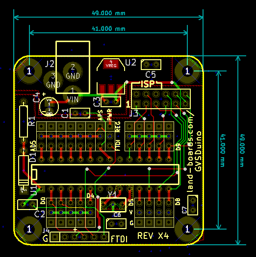
Board Dimensions
The board size is 49mm x 49mm.
The mounting holes are sized to support 4-40 or M3 screws.
3D Printed Open Frame
Gvsduino framed.png
GVSDuino-3D-Case.PNG
Factory Test
Equipment Used
- (2) LED-Test or LED-TEST-2 cards
- Cable set
- Wires D2-D13 and A0-A5 to LEDs
- Screwduino Test software
- Voltmeter
- Unit Under Test (UUT)
Test Procedure
- Install PWR jumper onto REG DC (J2) pins
- Install APS jumper onto VREF=5V pins
- Power card at DC jack J2 at 9V
- Check DC power at D0 (pin 1 = GND, pin 2 = VCC) using Voltmeter
- Result should be 4.90 to 5.10 V.
- Unplug power jack
- Move PWR jumper onto FTDI pins
- Attach FTDI cable at FTDI connector noting Ground position
- Attach LED test cards
- Plug in FTDI to/ USB from computer in
- Download Screwduino_test.ino to the UUT and run
- LEDs should all blink in order
- Download Blink sketch and run
- D13 LED should blink
- Disconnect USB host
- Mark test block on board rear
Past Revisions
GVSDuino Rev X8
X7 and X8 are identical but the netlist was updated to include the resonator.
Rev X7 had the same connections already present.
kiCompNL.py output - X7 vs X8
First netlist: GVSDuino-X7\GVSDuino.net
Number of Nets: 34
Second netlist: GVSDuino\GVSDuino.net
Number of Nets: 34
Extra pin(s) in net (2): RES0 pin(s) ['Y1-1']
Extra pin(s) in net (2): RES1 pin(s) ['Y1-3']
Extra pin(s) in net (2): ND pin(s) ['Y1-2']
GVSDuino Rev X7
kiCompNL.py output - X7 vs X6
First netlist: GVSDuino.net
Number of Nets: 34
Second netlist: GVSDuino-X6\GVSDuino-X6.net
Number of Nets: 35
net is in 1 but not 2 ['Net-(C5-Pad1)', 'C5-1']
Extra pin(s) in net (2): VREG pin(s) ['C5-1']
GVSDuino Rev X6 (vs X5)
kiCompNL.py output
First netlist: GVSDuino-X5.net
Number of Nets: 35
Second netlist: GVSDuino-X6.net
Number of Nets: 34
Mismatch in net (1): RES0 diff ['Y1-1']
Mismatch in net (1): VREG diff ['C5-1']
Mismatch in net (1): RES1 diff ['Y1-3']
Mismatch in net (1): ND diff ['Y1-2']
net is in 2 but not 1 ['Net-(C5-Pad1)', 'C5-1']
GVSDuino Rev X5
First netlist: C:\Users\doug_000\Documents\GitHub\lb-boards\GVSDuino\GVSDuino-X5\GVSDuino-X5.net
Number of Nets: 34
Second netlist: C:\Users\doug_000\Documents\GitHub\lb-boards\GVSDuino\GVS-Duino-X4\GVSDuino-X4.net
Number of Nets: 34
net is in 1 but not 2 ['/FTDIRES', 'C2-1', 'J4-6']
net is in 1 but not 2 ['/RESET', 'U1-1', 'C2-2', 'R1-2', 'D1-1', 'J3-5']
net is in 1 but not 2 ['d3)"', 'J1-3', 'J4-3']
net is in 1 but not 2 ['GND', 'K19-1', 'K18-1', 'K20-1', 'K17-1', 'J3-6', 'C7-2', 'C6-2', 'K13-1',
'C1-2', 'J4-2', 'J4-1', 'K4-1', 'U2-1', 'C3-2', 'C5-2', 'U1-22', 'U1-8', 'K3-1', 'K11-1', 'K5-1',
'K6-1', 'K12-1', 'K2-1', 'K1-1', 'K15-1', 'K16-1', 'K7-1', 'K8-1', 'K9-1', 'K10-1', 'K14-1', 'J2-3',
'J2-2', 'Y1-2', 'C4-2']
net is in 2 but not 1 ['/ARDRES', 'J4-6', 'J3-5', 'C2-1']
net is in 2 but not 1 ['""', 'K3-2', 'K4-2', 'K2-2', 'K1-2', 'K6-2', 'K21-2', 'K5-2']
net is in 2 but not 1 ['""', 'J1-3', 'J4-3']
net is in 2 but not 1 ['""', 'R1-2', 'C2-2', 'D1-1', 'U1-1']
GVSDuino Rev X4
ISP connector didn't work
RESET line on the ISP connector goes to the wrong side of the reset capacitor
Cut trace ARDRES U1-5 and U1-6 on rear of board
Add wire U1-1 to J3-5 (signal is new RESET line)
Rework worked
GVSDuino_X4_REWORK
GVSDuino Rev X3
GVSDuino Rev X3 is a fantastic card but we wanted to change a couple of things.

We wanted to be able to use an ISP cable to directly program the card.
The pinout of the ISP connector was intended for the ATProgHead design which had a difference on the reset/D10 pin.
We also wanted to connect up the extra pins on the extended header.
We wanted to add the land-boards.com web address onto the card.
GVSDuino Revision X3 is documented here.
GVSDuino Rev X2
GVSDuino Revision X2 is documented here.
GVSDuino Rev X1
GVSDuino Revision X1 is documented here.

