RASPI-PLUS-GVS-CFG
Contents
- 1 Features
- 2 Configuration EEPROM
- 3 3.3V Connectors
- 3.1 Raspberry Pi B Plus GPIO Connector
- 3.1.1 I2C bus
- 3.1.2 UART I/F
- 3.1.3 IO_4 GVS
- 3.1.4 IO_18 GVS
- 3.1.5 IO_17 GVS
- 3.1.6 IO_27 GVS
- 3.1.7 IO_23 GVS
- 3.1.8 IO_22 GVS
- 3.1.9 IO_24 GVS
- 3.1.10 IO_25 GVS
- 3.1.11 SPI0 (Serial Peripheral Interface)
- 3.1.12 SPI1 (Serial Peripheral Interface)
- 3.1.13 IO_5 GVS
- 3.1.14 IO_6 GVS
- 3.1.15 IO_12 GVS
- 3.1.16 IO_13 GVS
- 3.1.17 IO_19 GVS
- 3.1.18 IO_16 GVS
- 3.1.19 IO_26 GVS
- 3.1.20 IO_20 GVS
- 3.1.21 IO_21 GVS
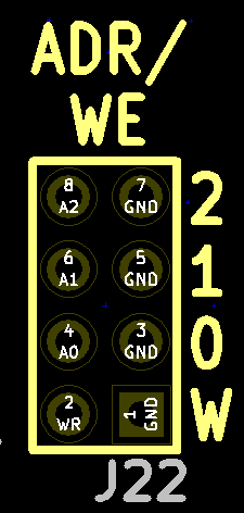
- 3.1.22 J22 - EEPROM Address/Write Enable Header - Rev X2 Hat
- 3.1.23 J22 - EEPROM Address/Write Enable Header - Rev X1 Hat
- 3.1.24 J23 - Voltage translator, 3V side
- 3.2 5V Connectors
- 3.1 Raspberry Pi B Plus GPIO Connector
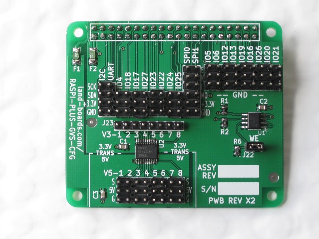
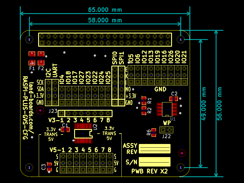
- 4 Layout - Rev X2
- 5 Layout - Rev X1
- 6 Assembly Sheet
- 7 Design Validation Testing - Rev X1 Board
- 8 Drivers/Example Code
- 9 Assembly Sheet
Features
- All Raspberry Pi I/O lines
- 8-bit bidirectional 3.3V to 5V level translator
- Configuration EEPROM
- Fuses on power
Raspberry Pi I/O lines
- All of the Raspberry Pi Model B+ I/O connections are brought to GVS connectors. This is:
- (17) GPIO lines on GVS connectors
- (2) SPI interfaces
- (1) UART interface
- (1) I2C interface
Level translators
- The BBB-GVS board use an 8-bit wide Texas Instrument TXS0108 voltage translator to convert up to 8 of the 3.3V I/O lines to 5V I/O levels.
Voltage Translators Features
- No Direction-Control Signal Needed
- Max Data Rates
- 60 Mbps (Push Pull)
- 2 Mbps (Open Drain)
- 1.2 V to 3.6 V on A Port and 1.65 V to 5.5 V on
- B Port (VCCA ≤ VCCB)
- No Power-Supply Sequencing Required –
- Either VCCA or VCCB Can Be Ramped First
- Latch-Up Performance Exceeds 100 mA Per JESD 78, Class II
- ESD Protection Exceeds JESD 22 (A Port)
- 2000-V Human-Body Model (A114-B)
- 150-V Machine Model (A115-A)
- 1000-V Charged-Device Model (C101)
- IEC 61000-4-2 ESD (B Port)
- ±6-kV Air-Gap Discharge
- ±8-kV Contact Discharge
Voltage Translators Architecture
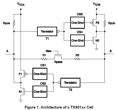
The TXS0108E can be used in level-translation applications for interfacing devices or systems operating at different interface voltages with one another. The TXS0108E is ideal for use in applications where an open-drain driver is connected to the data I/Os. The TXS0108E can also be used in applications where a push-pull driver is connected to the data I/Os, but the TXB0104 might be a better option for such push-pull applications. The TXS0108E device is a semi-buffered auto-direction-sensing voltage translator design is optimized for translation applications (e.g. MMC Card Interfaces) that require the system to start out in a low-speed open-drain mode and then switch to a higher speed push-pull mode.
To address these application requirements, a semi-buffered architecture design is used and is illustrated above (see Figure 1). Edge-rate accelerator circuitry (for both the high-to-low and low-to-high edges), a High-Ron n-channel pass-gate transistor (on the order of 300 Ω to 500 Ω) and pull-up resistors (to provide DC-bias and drive capabilities) are included to realize this solution. A direction-control signal (to control the direction of data flow from A to B or from B to A) is not needed. The resulting implementation supports both low-speed open-drain operation as well as high-speed push-pull operation.
When transmitting data from A to B ports, during a rising edge the One-Shot (OS3) turns on the PMOS transistor (P2) for a short-duration and this speeds up the low-to-high transition. Similarly, during a falling edge, when transmitting data from A to B, the One-Shot (OS4) turns on NMOS transistor (N2) for a short-duration and this speeds up the high-to-low transition. The B-port edge-rate accelerator consists of one-shots OS3 and OS4, Transistors P2 and N2 and serves to rapidly force the B port high or low when a corresponding transition is detected on the A port.
When transmitting data from B to A ports, during a rising edge the One-Shot (OS1) turns on the PMOS transistor (P1) for a short-duration and this speeds up the low-to-high transition. Similarly, during a falling edge, when transmitting data from B to A, the One-Shot (OS2) turns on NMOS transistor (N1) for a short-duration and this speeds up the high-to-low transition. The A-port edge-rate accelerator consists of one-shots OS1 and OS2, Transistors P1 and N1 components and form the edge-rate accelerator and serves to rapidly force the A port high or low when a corresponding transition is detected on the B port.
Fuses
- The board has Resettable fuses on the 3.3V and 5V from the Raspberry Pi.
- These fuses protect your Raspberry Pi from overloads.
- These fuses are 1/2 Amp PTC fuses.
- PTC fuses have certain advantages (they are self healing) and disadvantages (they are not like a wire fuse which acts like a switch).
- If you trust your wiring you may choose to solder a wire over the fuse.
- Care should be taken when doing so.
Configuration EEPROM
- The card has a Raspberry Pi Model B+ configuration EEPROM.
3.3V Connectors
The following are all 3.3VDC connections.
Raspberry Pi B Plus GPIO Connector
- J8 on the Pi.
I2C bus
- GND
- 3.3V
- SDA
- SCL
UART I/F
- GND
- 3.3V
- TxD
- RxD
IO_4 GVS
- GND
- 3.3V
- GPIO_4
IO_18 GVS
- GND
- 3.3V
- GPIO_18
IO_17 GVS
- GND
- 3.3V
- GPIO_17
IO_27 GVS
- GND
- 3.3V
- GPIO_27
IO_23 GVS
- GND
- 3.3V
- GPIO_23
IO_22 GVS
- GND
- 3.3V
- GPIO_22
IO_24 GVS
- GND
- 3.3V
- GPIO_24
IO_25 GVS
- GND
- 3.3V
- GPIO_25
SPI0 (Serial Peripheral Interface)
- GND
- 3.3V
- MOSI
- MISO
- SCK
- CE0
SPI1 (Serial Peripheral Interface)
- GND
- 3.3V
- MOSI
- MISO
- SCK
- CE1
IO_5 GVS
- GND
- 3.3V
- GPIO_5
IO_6 GVS
- GND
- 3.3V
- GPIO_6
IO_12 GVS
- GND
- 3.3V
- GPIO_12
IO_13 GVS
- GND
- 3.3V
- GPIO_13
IO_19 GVS
- GND
- 3.3V
- GPIO_19
IO_16 GVS
- GND
- 3.3V
- GPIO_16
IO_26 GVS
- GND
- 3.3V
- GPIO_26
IO_20 GVS
- GND
- 3.3V
- GPIO_20
IO_21 GVS
- GND
- 3.3V
- GPIO_21
J22 - EEPROM Address/Write Enable Header - Rev X2 Hat
- Write Enable - Install header to allow writes to EEPROM
- Remove header to protect EEPROM contents from accidental writes
J22 - EEPROM Address/Write Enable Header - Rev X1 Hat
- 1-2 = Write Enable - install to allow writes
- 3-4 = A0 - installed = 0
- 5-6 = A1 - installed = 0
- 7-8 = A2 - installed = 0
J23 - Voltage translator, 3V side
- V3-1 = Bit 1
- V3-2 = Bit 2
- V3-3 = Bit 3
- V3-4 = Bit 4
- V3-5 = Bit 5
- V3-6 = Bit 6
- V3-7 = Bit 7
- V3-8 = Bit 8
5V Connectors
The following are 5V connectors.
V5-1 - GVS connector, 5V side
- Ground
- +5V
- Bit1
V5-2 - GVS connector, 5V side
- Ground
- +5V
- Bit2
V5-3 - GVS connector, 5V side
- Ground
- +5V
- Bit3
V5-4 - GVS connector, 5V side
- Ground
- +5V
- Bit4
V5-5 - GVS connector, 5V side
- Ground
- +5V
- Bit5
V5-6 - GVS connector, 5V side
- Ground
- +5V
- Bit6
V5-7 - GVS connector, 5V side
- Ground
- +5V
- Bit7
V5-8 - GVS connector, 5V side
- Ground
- +5V
- Bit8
Layout - Rev X2
Kickstarter Edition
Layout - Rev X1
Prototype Edition - Not available on Kickstarter
RasPi-GVS-Plus-CFG-mechs.png
Assembly Sheet
RasPi-Plus-GVS-Cfg Configuration Sheet - Rev X2
Design Validation Testing - Rev X1 Board
RASPI-PLUS-GVS-CFG DVT
Factory Acceptance Tests (FAT)
Hardware
- FAT requires the following:
- Raspberry Pi Model B+ or equivalent (RasPi)
- Power supply for Raspberry Pi (5V at 1 Amp min) with Micro USB connector
- Monitor, Keyboard or Ethernet cable and laptop running puTTY
- Test Software loaded onto RasPi
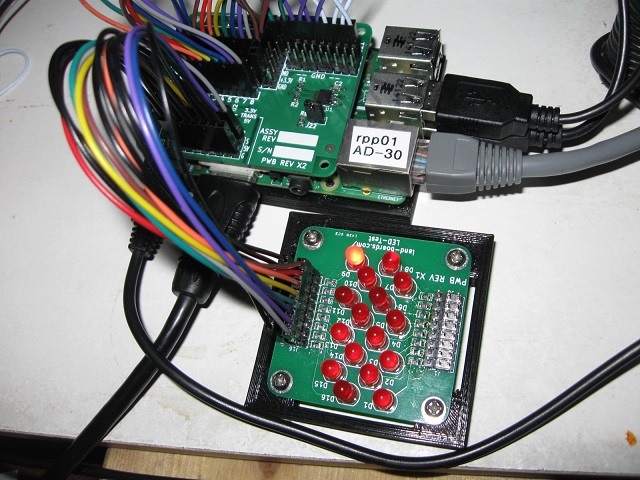
- (1) LED-Test card
- + side of LEDs to V5-2 thru 8
- - side of LEDs to GND at +5V side
- Jumpers (female-to-female)
- Daisy-chain cables
- 8-pin, 1-2, 3-4, 5-6, 7-8 @ IO6-IO21
- (2) 4-pin, 1 open, 2 open, 3-4 @ J1, J2
- Single female to female @ SPI1-IO5
- 6 pin, 1 open, 2 open, 3-4, 5-6 @ SPI0
- (3) 8-pin female-female jumper cables
- 1 jumper +3.3V side to IO4-IO25
- 2 (to LED-Test card)
- Unit Under Test (UUT)
Preliminary
- Install UUT onto RasPi
- Install Cables
- Power up card
- Log into RasPi
GVS Connector - Daisy-chain Tests
- On RasPi console:
pi
raspberry

cd ~/RasPi/RasPi-Plus-GVS-Cfg/
sudo python fastTests.py
- Result should be
Daisy test passed
- LEDs should cycle
I2C
cd ~/RasPi/RasPi-Plus-GVS-Cfg/eeprom/
sudo ./eep2flash.sh -w -t=24c32 -f=eepcfg.eep
sudo ./eep2flash.sh -r -t=24c32 -f=myeep.eep
rm stuff.eep
./eepdump myeep.eep stuff.eep
more stuff.eep | grep vendor

Verify:
# ---------- Dump generated by eepdump handling format version 0x01 ----------
#
# --Header--
# signature=0x69502d52
# version=0x01
# reserved=0
# numatoms=2
# eeplen=117
# ----------


# Start of atom #0 of type 0x0001 and length 57
# Vendor info
product_uuid 3ea7c89f-353e-4633-bd6c-2572996f277b
product_id 0x0004
product_ver 0x0001
vendor "land-boards.com"   # length=15
product "RASPI-PLUS-GVS-CFG"   # length=18
# End of atom. CRC16=0x437a


# Start of atom #1 of type 0x0002 and length 32
# GPIO map info
gpio_drive 0
gpio_slew 0
gpio_hysteresis 0
back_power 0
#        GPIO  FUNCTION  PULL
#        ----  --------  ----
# End of atom. CRC16=0x6eed
- Combined copy/paste
cd ~/RasPi/RasPi-Plus-GVS-Cfg/eeprom/ sudo ./eep2flash.sh -w -t=24c32 -f=eepcfg.eep sudo ./eep2flash.sh -r -t=24c32 -f=myeep.eep rm stuff.eep ./eepdump myeep.eep stuff.eep diff stuff.eep eepcomp.eep cd ~/RasPi/RasPi-Plus-GVS-Cfg/ sudo python fastTests.py== Schematic ==Drivers/Example Code
* Github repo - Driver codeAssembly Sheet
* RASPI-PLUS-GVS-CFG Assembly Sheet

