SIMPLE-68008
Jump to navigation
Jump to search
Contents
- 1 Features
- 2 Design
- 3 Headers / Connectors
- 4 SIMPLE-68008 Software
- 4.1 Linux Development Environment
- 4.2 Initial Test Code
- 4.3 68k-Monitor
- 4.4 Example Assembly Code
- 4.5 Example C Code
- 4.6 String Test C Code
- 4.7 Test Transmit Interrupt Code
- 4.8 Receive Interrupt Test Code
- 4.9 60 Hz timer
- 4.10 Guess a Number Game Code
- 4.11 Sample Game with ANSI screen control
- 4.12 Sample Game
- 4.13 First Person Shooter Game
- 4.14 Enhanced BASIC (Running from SRAM)
- 4.15 68K Monitor Plus Enhanced BASIC (Running from ROM)
- 4.16 68000 fig-FORTH V1.0
- 5 Mechanicals
- 6 Checkout
- 7 Assembly Sheet
Features
- 68008 CPU
- 20 bit address space (1MB total)
- 10 MHz clock
- 128KB/512KB SRAM
- Runs with zero wait states
- Up to 448KB EPROM/EEPROM
- Runs with zero wait states
- 68681 Dual Serial Port (ACIA)
- Headers for FTDI
- 38,400 baud (other rates are programmable)
- Connected to FTDI-49MM card
- FTDI-49MM card drives 5V to the card
- Run serial terminal program on the PC
- Reset switch with optional Power Supervisor
- 5V operation
- 375 mA nominal
- 95x95mm card
- (4) 6-32 mounting holes
Memory Map
- 0x00000-0x7FFFF 512KB SRAM
- 0x80000-0xEFFFF Up to 448KB EPROM (minus DUART I/O space)
- 0x80000 write with D0 = 1 to unmap the EPROM from the SRAM space
- 0x80000-0x87FFF 27C256 (322KB)
- 0x80000-0x8FFFF 27C512 (64KB)
- 0xF0000-0xFFFFF Serial (ACIA)
Alternate Memory Map
- Other memory maps could be done
- For instance, the Teeside memory map could be used
- The memory map depends on two things
- Mapping in the PLDs
- The firmware that is being run on the card has to match the memory map
Chip Set
- On Ebay
- $20 plus $9 shipping (2024-08)
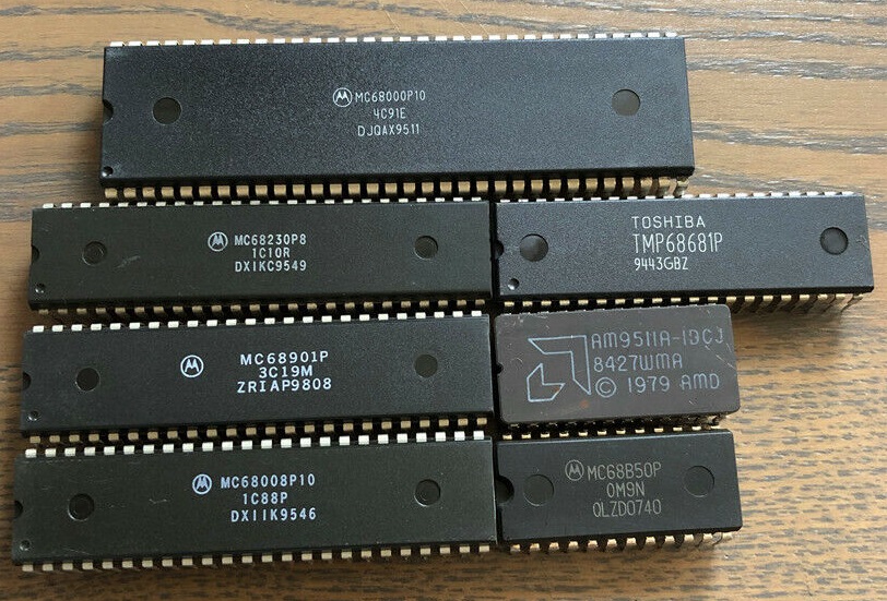
Parts in "Kit"
- Only the MC68000P10 and TMP68681P are used by this card
- MC68000P10 - 68K CPU with 16-bit data bus and 24-bit address bus
- TMP68681P - Dual UART, 8-bit I/O, 6-bit I/O
- MC68230P8 - Parallel I/O bits, timer
- MC68901P - Multifunction (8 I/O pins, interrupt controller, (4) timers, UART
- AM8511A - Floating Point Unit
- MC68008P10 - 68K CPU with 8-bit data bus and 20-bit address bus
- 65B50P - ACIA (Serial interface)
Design
CPU
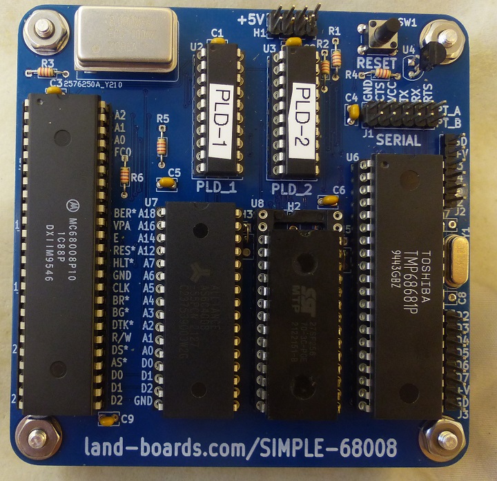
- The Motorola 68008 is an 8/32-bit microprocessor introduced by Motorola in 1982
- It is a version of 1979's Motorola 68000 with an 8-bit external data bus, as well as a smaller address bus
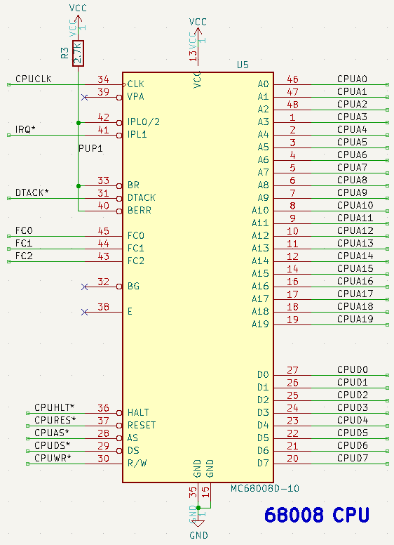
- This card uses a 68008 with 20 address lines (48-pin package) which allowed 1 MB address space versus the 16 MB addressable on the 68000
- Rev 1 needs a wire jumper U5-39 to U5-40 to pull up VPA*
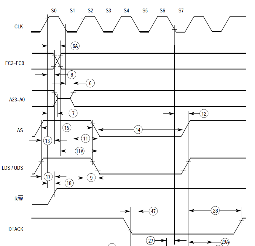
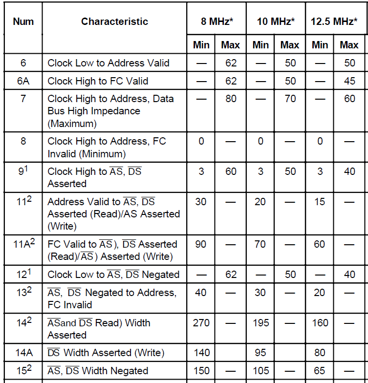
CPU Timing
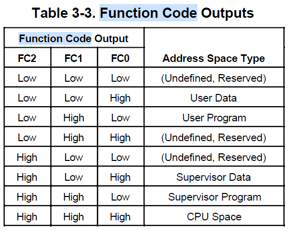
Function Code
EPROM
- Program using TL-866ii plus programmer
- SST27C256 EEPROM
- 32 KB part
- 28 pin part, 32 pin socket
- SST27C512 EEPROM
- 64 KB part
- 28 pin part, 32 pin socket
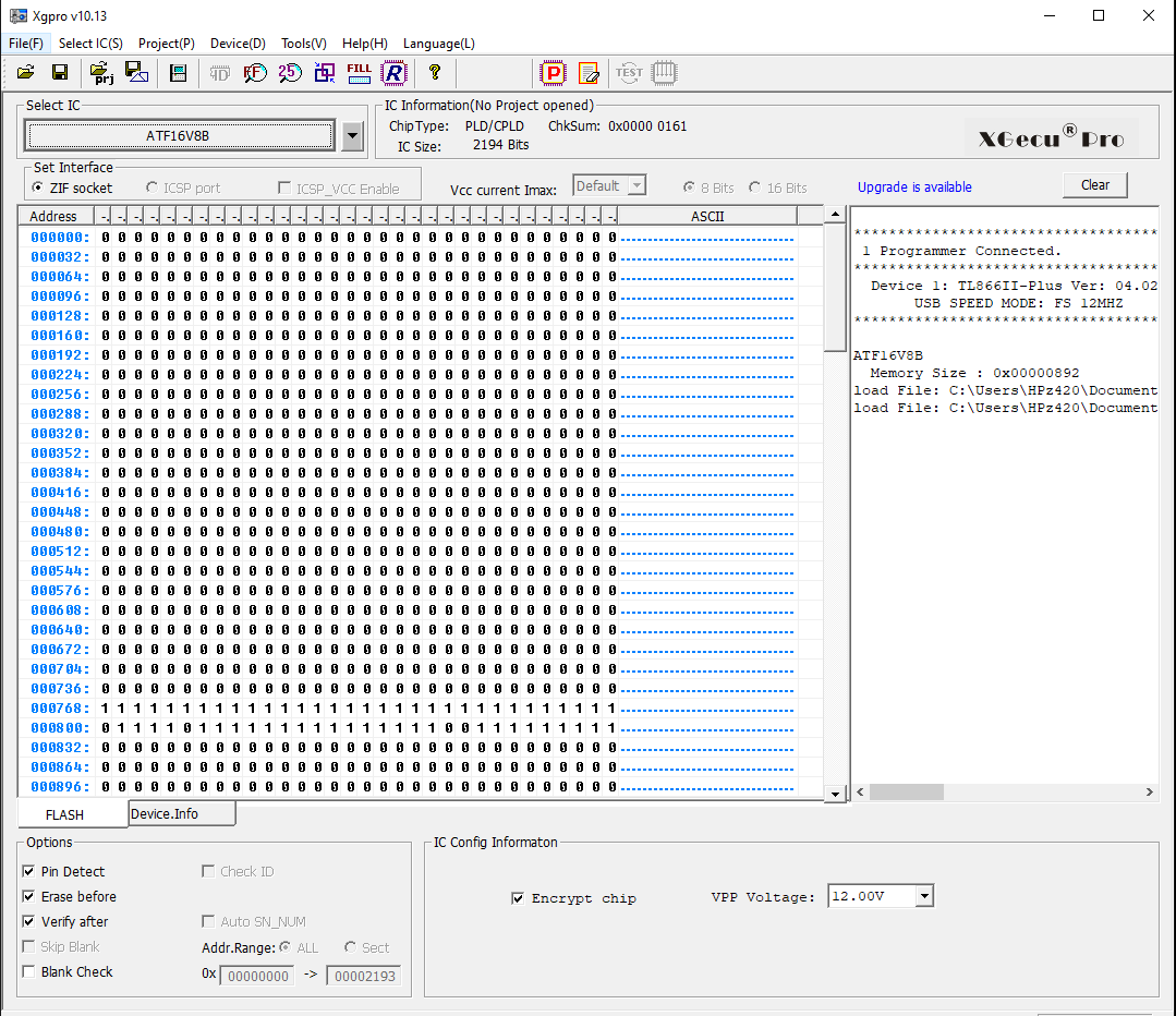
Flash Memory (EEPROM) Programming
- Program using TL-866ii plus programmer
- Select device type
- File Open
- Select file = S68K_001.hex
- File format: INTEL_HEX
- To Region: Default
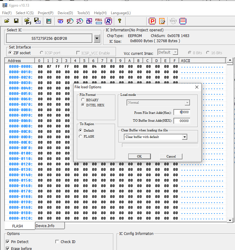
- Set EPROM offset when file is loaded to accommodate memory map offsets for EPROM space
- Set From File Start Addr(Hex) to 80000
- To Buffer Start Addr(Hex) to 00000 (should be already that value)
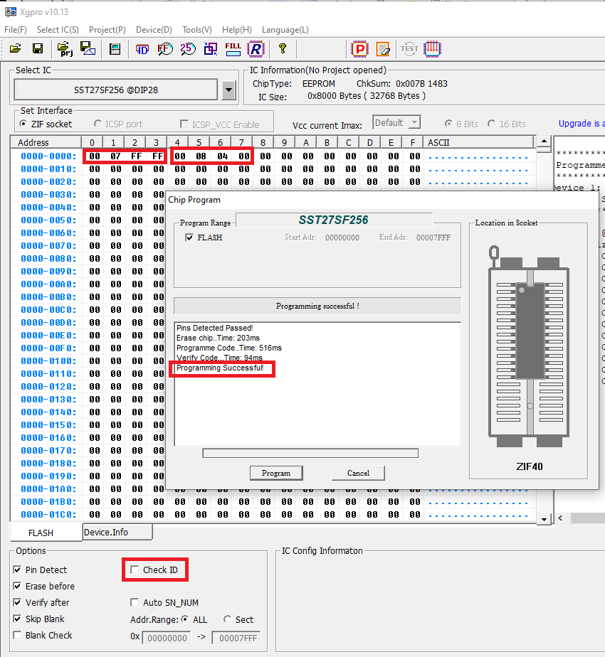
- Got Device ID error
- Turn off ID checkbox in the Options section (bottom left of window)
- Using SST 27SF512 part (Part is 64 KB)
- Parts are actually Winbond parts remarked as SST
- Looking up device ID showed the parts are actually Winbond parts
- Can set programmer to Winbond part and it programs without error
- Device programmed/verified
- Memory Buffer should look like
Device ID Mysteries
- Ebay has parts with SST marking
- EPROM Programmer says the parts are WinBond (Manufacturer ID 0xDA)
- Part marked as 27SF512 and it's a 27C512 (Part ID 0x08)
- Windbond 27C512 qty 10 are cheaper than SST part on ebay
SRAM
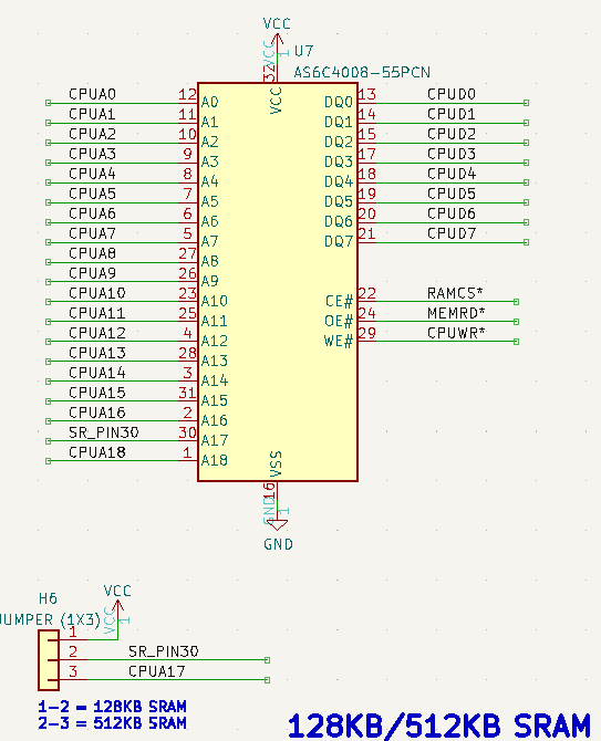
- Using 512 KB SRAM
- Wire jumper H6-2 to H6-3 on rear of card
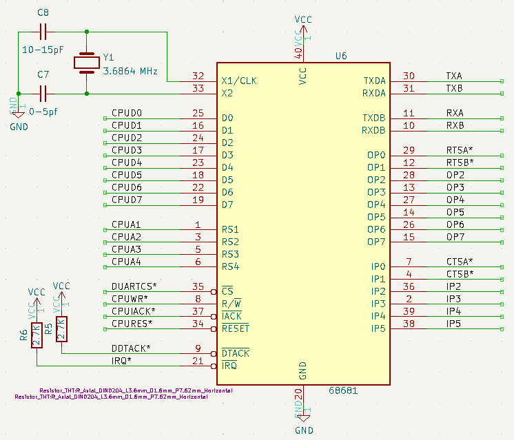
Dual UART
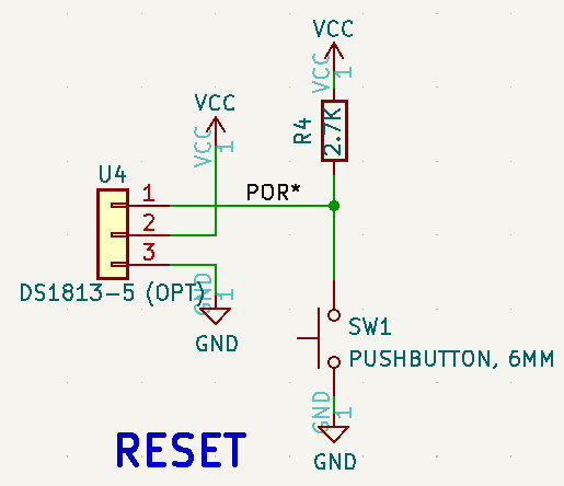
Reset
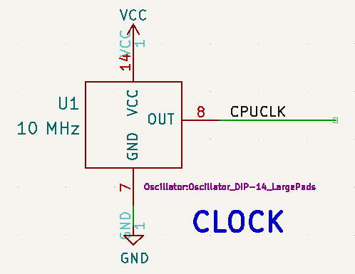
Clock
- Test and works with 8 MHZ and 10 MHz crystal oscillator
PLDs
- Two ATF16V8B PLDs (Datasheet)
- WinCupl compiler used to write PLD "code"
- Program using TL-866ii plus programmer
- Part = ATF16V8B
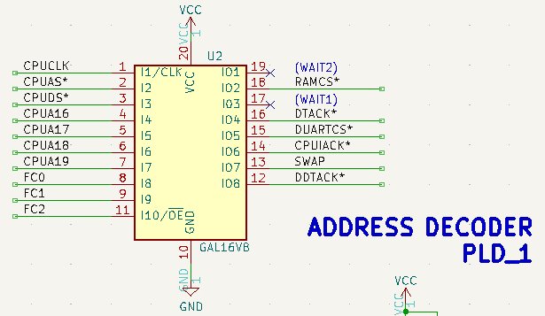
PLD_001
PLD_001 Source Listing
- Source file
- JEDEC Programming file
- WAIT1 and WAIT2 are not used since the DUART has a DTACK* out and the EPROM/SRAM run at zero wait states
Name       SIMPLE-68008_PLD_1;
Partno     ATF16V8B;
Date       07/13/24;
Revision   01;
Designer   DOUG G;
Company    LAND BOARDS LLC;
Assembly   U02;
Location   RUSTBELT, USA;
Device     G16V8;

/*
*/

/* Inputs */
PIN    1   = CLK;
PIN    2   = !CPUAS;
PIN    3   = !CPUDS;
PIN    4   = CPUA16;
PIN    5   = CPUA17;
PIN    6   = CPUA18;
PIN    7   = CPUA19;
PIN    8   = CPUFC0;
PIN    9   = CPUFC1;
PIN    11  = CPUFC2;
PIN    12  = !DDTACK;
PIN    13  = SWAP;

/* Outputs */
PIN    14  = !CPUIACK;
PIN    15  = !DUARTCS;
PIN    16  = !CPUDTACK;
PIN    17  = WAIT1;
PIN    18  = !RAMSEL;
PIN    19  = WAIT2;

CPUIACK = CPUA19 & CPUA18 & CPUA17 & CPUA16 & CPUFC2 & CPUFC1 & CPUFC0 & CPUDS;

DUARTCS = CPUA19 & CPUA18 & CPUA17 & CPUA16 & CPUDS & !CPUFC1 &  CPUFC0;

RAMSEL = !CPUA19 & SWAP & CPUDS & !CPUFC1 &  CPUFC0  		/* User/Super Data */
#        !CPUA19 & SWAP & CPUDS &  CPUFC1 & !CPUFC0; 		/* User/Super Program */

CPUDTACK = CPUA19 & CPUA18 & CPUA17 & CPUA16 & CPUDS & !CPUFC1 & CPUFC0 & DDTACK		/* DUART Data spaces	*/
#	    CPUA19 & CPUA18 & CPUA17 & CPUA16 & CPUDS & CPUFC2 & CPUFC1 & CPUFC0 & DDTACK	/* DUART IACK space */
#          CPUA19 & !CPUA18 & CPUDS								/* EPROM	*/
#          CPUA19 & !CPUA17 & CPUDS								/* EPROM	*/
#          CPUA19 & !CPUA16 & CPUDS								/* EPROM	*/
#          !CPUA19 & CPUDS;									/* RAM 		*/
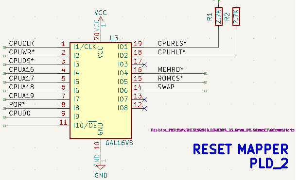
PLD_002
- The SWAP line maps the EPROM to the SRAM space
- EPROM map addresses still work and are mapped to 0x8000-0xEFFFF
- Used to pull the Stack pointer and start address from EPROM
- Set to 0 at power up
- Write to address 0x80000 with D0 = 1 to unmap the EPROM from the SRAM space
- Needs to be set early in the startup code before SRAM is accessed
PLD_002 Source Listing
Name       SIMPLE-68008_PLD_2;
Partno     ATF16V8B;
Date       06/19/24;
Revision   01;
Designer   DOUG G;
Company    LAND BOARDS LLC;
Assembly   U03;
Location   RUSTBELT, USA;
Device     G16V8;

/*
	RESET CONTROLLER, ROM CHIP SELECT
*/

/* Inputs */
PIN    1   = CLK;
PIN    2   = !CPUWR;
PIN    3   = !CPUDS;
PIN    4   = CPUA16;
PIN    5   = CPUA17;
PIN    6   = CPUA18;
PIN    7   = CPUA19;
PIN    8   = !POR;
PIN    9   = CPUD0;

/* Outputs */
PIN	  13  = SWAPADR;
PIN    14  = SWAP;
PIN    15  = !ROMCS;
PIN    16  = !MEMRD;
PIN    18  = !CPUHLT;
PIN    19  = !CPURES;

/* CLEAR SWAP AT POWER UP, RESET	*/
/* SET SWAP BY 1ST WR TO START OF EPROM SPACE		*/
/* SWAP.CK = CLK; */
/* SWAP.AR = POR; */

MEMRD = !CPUWR & CPUDS & !CPUA19
#       !CPUWR & CPUDS &  CPUA19 & !CPUA18
#       !CPUWR & CPUDS &  CPUA19 & !CPUA17
#       !CPUWR & CPUDS &  CPUA19 & !CPUA16;

SWAP = CPUDS &  CPUWR & CPUA19 & !CPUA18 & !CPUA17 & !CPUA16 & CPUD0 & !POR
#      SWAP  & !POR;

SWAPADR = CPUDS & CPUWR & CPUA19 & !CPUA18 & !CPUA17 & !CPUA16;

ROMCS = CPUDS & !CPUWR & CPUA19 & !CPUA18
#       CPUDS & !CPUWR & CPUA19 & !CPUA17
#       CPUDS & !CPUWR & CPUA19 & !CPUA16
#       CPUDS & !CPUA19 & !CPUA18 & !CPUA17 & !CPUA16 & !SWAP;

CPUHLT.OE = POR;
CPUHLT = POR;

CPURES.OE = POR;
CPURES = POR;
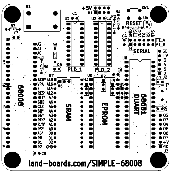
Headers / Connectors
J1 - 2 port FTDI / TTL Serial
- 2x6 header
- Direct connect to DTE RS-232 card
- Flip order to connect to USB to TTL Serial (FTDI)
- TX<>RX
- RTS<>CTS
- Pinout
- GND
- CTS* (in)
- +5V
- Transmit (out)
- Receive (in)
- RTS* (out)
Connections to ESP32-TERM Card
- ESP32-TERM card
| ESP32-TERM | SIMPLE-68008 | |||
|---|---|---|---|---|
| Pin | Signal | Pin | Signal | |
| 1 | GND | 1 | GND | |
| 2 | RTS (out) | 2 | CTS (in) | |
| 3 | +5V | 3 | +5V | |
| 4 | RX (in) | 4 | TX (out) | |
| 5 | TX (out) | 5 | RX (in) | |
| 6 | CTS (in) | 6 | RTS (out) |
J2 - Input Port
- Input 2
- Input 5
- Input 4
- Input 3
- Vcc
- GND
J3 - Output Port
- GND
- Vcc
- Output 7
- Output 6
- Output 5
- Output 4
- Output 3
- Output 2
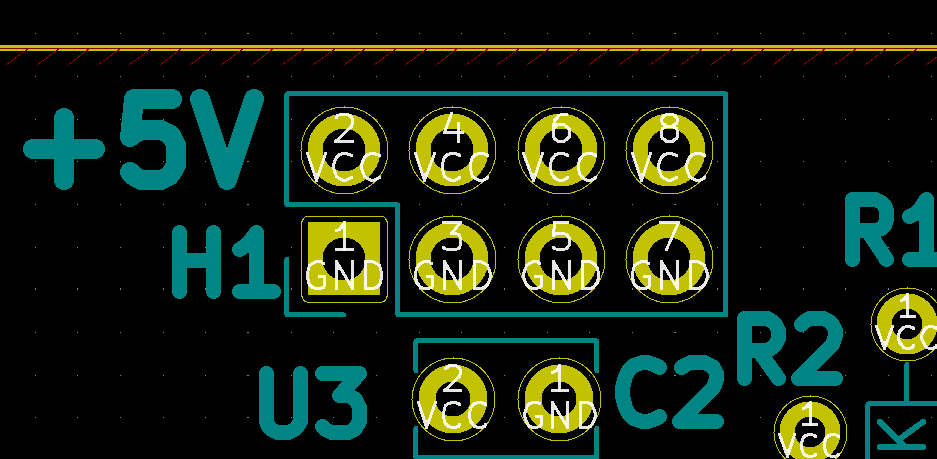
H1 - 5V Power
- 2x4 header
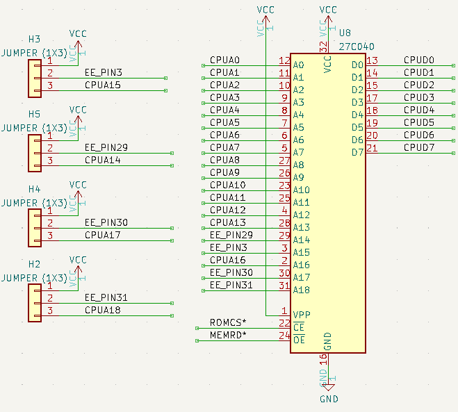
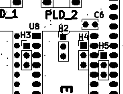
H2-H5 - EPROM/EEPROM Select Jumpers
- H2 = EE PIN 31
- H3 = EE PIN 3
- H4 = EE PIN 30
- H5 = EE PIN 29
27SF256
- 27SF256 is a 28 pin part, socket is 32 pins
- H2 = Not installed
- H3-2 to H3-3 = A15 (Vpp on 27SF256, but pin can be either high or low)
- H4-1 to H4-2 = Vcc
- H5-2 to H5-3 = CPUA14
EEPROM Jumpers
| 27040 | 27020 | 27010 | 27512 | 27256 | 27128 | 2764 | PIN(32) | PIN(28) | PIN(28) | PIN(32) | 2764 | 27128 | 27256 | 27512 | 27010 | 27020 | 27040 | |
|---|---|---|---|---|---|---|---|---|---|---|---|---|---|---|---|---|---|---|
| VPP | VPP | VPP | N/A | N/A | N/A | N/A | 1 | N/A | N/A | 32 | N/A | N/A | N/A | N/A | VCC | VCC | VCC | |
| A16 | A16 | A16 | N/A | N/A | N/A | N/A | 2 | N/A | N/A | 31 (H2) | N/A | N/A | N/A | N/A | PGM | PGM | A18 | |
| A15 | A15 | A15 | A15 | VPP | VPP | VPP | 3 (H3) | 1 | 28 | 30 (H4) | VCC | VCC | VCC | VCC | N/C | A17 | A17 | |
| A12 | A12 | A12 | A12 | A12 | A12 | A12 | 4 | 2 | 27 | 29 (H5) | PGM | PGM | A14 | A14 | A14 | A14 | A14 | |
| A7 | A7 | A7 | A7 | A7 | A7 | A7 | 5 | 3 | 26 | 28 | A13 | A13 | A13 | A13 | A13 | A13 | A13 | |
| A6 | A6 | A6 | A6 | A6 | A6 | A6 | 6 | 4 | 25 | 27 | A8 | A8 | A8 | A8 | A8 | A8 | A8 | |
| A5 | A5 | A5 | A5 | A5 | A5 | A5 | 7 | 5 | 24 | 26 | A9 | A9 | A9 | A9 | A9 | A9 | A9 | |
| A4 | A4 | A4 | A4 | A4 | A4 | A4 | 8 | 6 | 23 | 25 | A11 | A11 | A11 | A11 | A11 | A11 | A11 | |
| A3 | A3 | A3 | A3 | A3 | A3 | A3 | 9 | 7 | 22 | 24 | OE* | OE* | OE* | OE* | OE* | OE* | OE* | |
| A2 | A2 | A2 | A2 | A2 | A2 | A2 | 10 | 8 | 21 | 23 | A10 | A10 | A10 | A10 | A10 | A10 | A10 | |
| A1 | A1 | A1 | A1 | A1 | A1 | A1 | 11 | 9 | 20 | 22 | CE* | CE* | CE* | CE* | CE* | CE* | CE* | |
| A0 | A0 | A0 | A0 | A0 | A0 | A0 | 12 | 10 | 19 | 21 | D7 | D7 | D7 | D7 | D7 | D7 | D7 | |
| D0 | D0 | D0 | D0 | D0 | D0 | D0 | 13 | 11 | 18 | 20 | D6 | D6 | D6 | D6 | D6 | D6 | D6 | |
| D1 | D1 | D1 | D1 | D1 | D1 | D1 | 14 | 12 | 17 | 19 | D5 | D5 | D5 | D5 | D5 | D5 | D5 | |
| D2 | D2 | D2 | D2 | D2 | D2 | D2 | 15 | 13 | 16 | 18 | D4 | D4 | D4 | D4 | D4 | D4 | D4 | |
| GND | GND | GND | GND | GND | GND | GND | 16 | 14 | 15 | 17 | D3 | D3 | D3 | D3 | D3 | D3 | D3 |
H6 - SRAM Configuration
- 1-2 = 128KB SRAM
- 2-3 = 512KB SRAM
- 128KB and 512KB Parts are about the same price so there's not much point (if buying parts anyway) with going with 512KB part
- AS6C4008-55PCN is $6.38 (2024-06)
- AS6C1008-55PCN is $2.91 (2024-06)
SIMPLE-68008 Software
- SIMPLE-68008 Code Repository
- 68000 code development is done with cross assemblers/compilers using GCC tools under Linux
- 68000 Assembly Language YouTube Playlist
Linux Development Environment
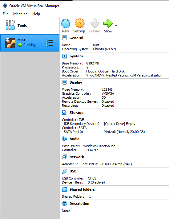
- Using Oracle VM VirtualBox
- Running Linux Mint
- The [m68k assembly code toolchain GNU C-Compiler with Binutils and other useful tools for 68000 cross development
- This is a Makefile based approach to build the toolchain to reduce the build time.
- The original work was by Steve Moody's page
- These tools are build:
- binutils
- gcc with libs for C/C++/ObjC
- vasm
- vbcc
- vlink
- newlib
S Record and Hex file manipulation
Initial Test Code
- S68K_001 - Test Code Repo
- Uses m68k assembly code toolchain
- Set up stack, starting address
- 68681 DUART code
- 9600 baud
- Initialize DUART
- Input/Output Serial routines
- Loop forever
68k-Monitor
- S68K_002 - Monitor Code Repo here
- Uses m68k assembly code toolchain
- Built from ChartreusK 68K monitor = 68901 DUART code
- Added S-Record load ('L' on command line)
- Runs at 38,400 baud with no waits/handshakes on transmit from Host Side
- Added improved SRAM test code
- Added SRAM fill
- Added 60 Hz timer code
- Added Serial port hardware handshake from notes
- Type 'T' to start timer
- Long word timer at 0x608-0x60b
- Can be used as random number value if code is run from SRAM since the lowest byte s/b continually updated
Monitor Commands
- L - Load S-Record
- R - Run program from SRAM
- E - Examines memory addresses
- E ADDR Displays a single byte
- E ADDR-ADDR Displays all bytes between the two addresses
- E ADDR+LEN Displays LEN bytes after ADDR
- E ADDR; Interactive mode, space shows 16 lines, enter shows 1.
- E ADDR. Quick line, displays one line
- D - Deposit values into RAM
- D ADDR VAL VAL Deposit value(s) into RAM
- D ADDR VAL VAL; Deposit values, continue with values on next line
- VAL VAL VAL; - Continuing with further continue
- d: VAL VAL Continue depositing values after the last address written to
Hardware Handshake Notes
- From this page
*       Set MR2A4 = 1 and MR2A5 = 1 to configure OP0 as RTS output
       MOVE.B #$83,MR1A
       MOVE.B #$27,MR2Aer is ready to
*       receive more data. Note also that the contents of the DUART's
*       output port register are inverted before they are fed to the output
*       pins. That is, to assert RTS* low, it is necessary to load a one
*       into the appropriate bit of the OPR.
*
       MOVE.B #$01,OPR Set OPR0 to assert RTS*
Example Assembly Code
- S68K_003 - Assembly Code Example Repo
- Uses m68k assembly code toolchain
- Runs out of SRAM
- Loops forever
- Blinks LED connected to O2 (red LED, 4.7K resistor, wired to ground)
- Load and run
SIMPLE-68008 CPU
RAM Test Passed
> L
Load S-Record
+++++>
> R1000
Example C Code
- S68K_004 - C Code Example Repo
- Uses m68k assembly code toolchain
- Runs out of SRAM
- Loops forever
- Blinks LED connected to O2 (red LED, 4.7K resistor, wired to ground)
- Load and run
SIMPLE-68008 CPU
RAM Test Passed
> L
Load S-Record
+++++>
> R2000
String Test C Code
- S68K_005 - C Code Example Repo
- Uses m68k assembly code toolchain
- ASCII code
- Runs out of SRAM
- Loops forever
- Blinks LED connected to O2 (red LED, 4.7K resistor, wired to ground)
- Load and run
SIMPLE-68008 CPU
RAM Test Passed
> L
Load S-Record
+++++>
> R2000
Test Transmit Interrupt Code
- S68K_006 - Interrupt Test Code Example Repo
- Uses m68k assembly code toolchain
- Runs out of SRAM
- Loops forever
- Sends out alphabet forever using Transmit interrupt from 68681
- Required jumper U5-39 to U5-40 to always pullup VPA* to Vcc
SIMPLE-68008 CPU V1.00
RAM Test Passed
> l
Load S-Record
++++++++++++++++++++>
> r1000
SIMPLE-68008 CPU V1.00
RAM Test Passed
> r1100
42345678S:;<I>?@ABMDPFGHLJKE-6O8QRS00VW8 Z[\C^_`PbUd fghijkVm1o.qrst0vwx0z2
]R7AM:; =>T@ABeDEsGt JKLPNaPsRSsUVWXed[ >` bcdefghijklmnopqrstuvwxyz
23456789:;<=>?@ABCDEFGHIJKLMNOPQRSTUVWXYZ[\]^_`abcdefghijklmnopqrstuvwxyz
23456789:;<=>?@ABCDEFGHIJKLMNOPQRSTUVWXYZ[\]^_`abcdefghijklmnopqrstuvwxyz
23456789:;<=>?@ABCDEFGHIJKLMNOPQRSTUVWXYZ[\]^_`abcdefghijklmnopqrstuvwxyz
23456789:;<=>?@ABCDEFGHIJKLMNOPQRSTUVWXYZ[\]^_`abcdefghijklmnopqrstuvwxyz
23456789:;<=>?@ABCDEFGHIJKLMNOPQRSTUVWXYZ[\]^_`abcdefghijklmnopqrstuvwxyz
Receive Interrupt Test Code
- S68K_007 GitHub Repository
- Test interrupt from DUART
- Using receive character interrupt
- Runs from RAM
- Echos back character typed
- Downloaded as S Records
- Loaded with L command in S68K_002 monitor
- R1000 to run program
60 Hz timer
- S68K_008 GitHub Repository
- Make a 60 Hz Counter in memory
- Use timer in DUART
- 3.6864 MHz / 16 = 23400
- 23,400 / 60 (Hz) / 2 per cycle = 1920 count = 0x780
- Increment a long in 0x604(-0x607)
- 60 Hz is 0x780 divisor
- Stop timer to clear timer
- Restart timer to set up interrupt on next timer edge
Guess a Number Game Code
- S68K_GAME_01
- Game to guess a number from 1-99
- Missing random number generator
- Structures string and DUART I/O code into separate files
- Game to guess a number from 1-99
- S68K_GAME_02
- Game to guess a number from 1-99
- Version adds random number generator
- Slightly less clumsy includes (added a main() stub and moved includes to right after that)
- Game to guess a number from 1-99
Sample Game with ANSI screen control
- S68K_GAME_03
- Move an object around the screen using arrow keys
- To load it into the S68K_002 monitor you can run the command "L" and then send the run (S record) .run file to the serial port
- Run the program from the S68K_002 monitor using R2000
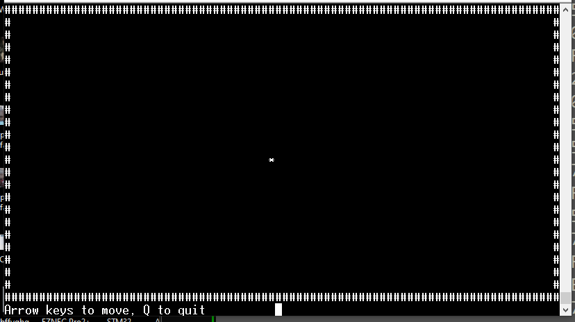
- Output should look like the following:
SIMPLE-68008 CPU

RAM Test Passed

 > l

Load S-Record

++++++++++++++++++++++++++++>

 > r2000
- Scrren should clear and a '*' will be at the center
- Arrow keys to move around the '*'
- Q to quit
ANSI Terminal Driver
- nncurses
- Similar to ncurses
- nncurses is not ncurses
- n curses is not curses
- nncurses is not ncurses
- Similar to ncurses
- Drive ANSI/VT terminal
- Double buffered implementation
- Write to fromBuffer[][]
- Copy to screenBuffer[][]
- Send out delta as ANSI sequences to the Serial Terminal
- ASCII code table
- ANSI.SYS
- ANSI/VY-xxx ESC sequences
Sample Game
- S68K_GAME_04
- Game framework with basic game elements
- Written in C
- Writes to ANSI screen
- Uses cursor position commands
- Draws border on the screen
- Status line at the bottom of the screen
- Puts '*' at center of the screen
- Arrow keys move '*' around the playfield
First Person Shooter Game
- S68K_GAME_06
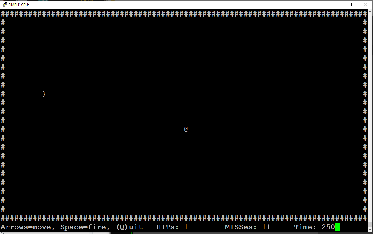
- Runs on ANSI/VT terminal
- First person shooter
- Scores of hits/misses
- Elapsed time since game start
- Target random movement based on modulo of timer
Enhanced BASIC (Running from SRAM)
- Lee Davidson's Enhanced BASIC
- 38,400 baud serial connection (monitor and BASIC)
- Running BASIC from card reset
SIMPLE-68008 CPU
RAM Test Passed
- L for Load
> l
Load S-Record
+++++++++++++++++++++++++++++++++++++++++++++++++++++++++++++++++++++++++++++++++++++++++++++++++++++++++
+++++++++++++++++++++++++++++++++++++++++++++++++++++++++++++++++++++++++++++++++++++++++++++++++++++++++
+++++++++++++++++++++++++++++++++++++++++++++++++++++++++++++++++++++++++++++++++++++++++++++++++++++++++
+++++++++++++++++++++++++++++++++++++++++++++++++++++++++++++++++++++++++++++++++++++++++++++++++++++++++
+++++++++++++++++++++++++++++++++++++++++++++++++++++++++++++++++++++++++++++++++++++++++++++++++++++++++
+++++++++++++++++++++++++++++++++++++++++++++++++++++++++++++++++++++++++++++++++++++++++++++++++++++++++
+++++++++++++++++++++++++++++++++++++++++++++++++++++++++++++++++++++++++++++++++++++++++++++++++++++++++
+++++++++++++++++++++++++++++++++++++++++++++++++++++++++++++++++++++++++++++++++++++++++++++++++++++++++
++++++++++++++++++++++++++++++++++++++++++++++++++++++++++>
- Run at 800
> R800
457232 Bytes free

Enhanced 68k BASIC Version 3.52

Ready
- Test with short program
10 PRINT "HI"
RUN
HI

Ready
68K Monitor Plus Enhanced BASIC (Running from ROM)
- This code puts S68K_002 - Monitor Code and Enhanced BASIC into a single 32KB ROM
- Build steps
- Run make for S68K_002
- Run make for the Enhanced BASIC which pulls in the S68K_002 code
- Result is a .hex file
- Boots into the monitor
- Run BASIC with 'B' on command line
- Runs at 38,400 baud
SIMPLE-68008 CPU V1.00
RAM Test Passed
> b
12
490032 Bytes free

Enhanced 68k BASIC Version 3.52

Ready
Monitor Commands
- H - Help
- B - Run Enhanced BASIC
- L - Load S-Record
- R - Run program from SRAM
- E - Examines memory addresses
- e ADDR Displays a single byte
- e ADDR-ADDR Dispalys all bytes between the two addresses
- e ADDR+LEN Dispays LEN bytes after ADDR
- e ADDR; Interactive mode, space shows 16 lines, enter shows 1.
- e ADDR. Quick line, displays one line
- D - Deposit values into RAM
- d ADDR VAL VAL Deposit value(s) into RAM
- d ADDR VAL VAL; Deposit values, continue with values on next line
- VAL VAL VAL; - Continuing with further continue
- d: VAL VAL Continue depositing values after the last address written to
Memory Map
- EPROM base address = 0x80000
- 0x80000-0x83FFF - First 16KB reserved addresses for monitor (plenty of room for expansion)
- Code is from 0x80400-0x80caf (Less than 4KB)
- 0x84000-0x87FFF - Second 16KB reserves addresses for BASIC (plenty of room for expansion)
- Code is from 0x84800-0x87D1F (Less than 16KB)
68000 fig-FORTH V1.0
- Source Repository
- Runs from SRAM
- Run at 3648
- From reset
SIMPLE-68008 CPU V1.00
RAM Test Passed
> l
Load S-Record
++++++++++++++++++++++++++++++++++++++++++++++++++++++++++++++++++++++++++++++++++++++++++++++++++++++
++++++++++++++++++++++++++++++++++++++++++++++++++++++++++++++++++++++++++++++++++++++++++++++++++++++
++++++++++++++++++++++++++++++++++++++++++++++++++++++++++++++++++++++++++++++++++++++++++++++++++++++
++++++++++++++++++++++++++++++++++++++++++++++++++++++++++++++++++++++++++++++++++++++++++++++++++++++
+++++++++++++++++++++++++++>
> r3648

68000 fig-FORTH V1.0
    OK
    OK
    OK
1 2 3     OK
+    OK
+    OK
. 6    OK
Mechanicals
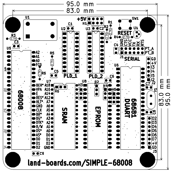
- Rev 1 card
Checkout
Rev 2 Card Checkout
- Ordered a batch of 10 cards (2024-08-18)
- Tested card, works!
Rev 2 Card Changes
- Fixed DUART TXB and RXA connections (see Rev 1 rework)
- Added pullup to VPA* line (to make interrupts work - see Rev 1 rework)
- Add some silkscreen annotations for memory configuration header connections to rear of card
- Moved R6 up and added more silkscreen near CPU
- Added R7 resistor and LED to ground on U3-12
- Access with a write of but D0 to EEPROM address (similar to SWAP bit)
Rev 1 Card
- VPA needs to be pulled up
- Add wire U5-39 to U5-40
- Reset working
- Reset switch and monitor working
- Clock working
- Checked at 8 and 10 MHz
- EPROM working
- SRAM working
- Checked Serial port
- Not using any XTAL capacitors
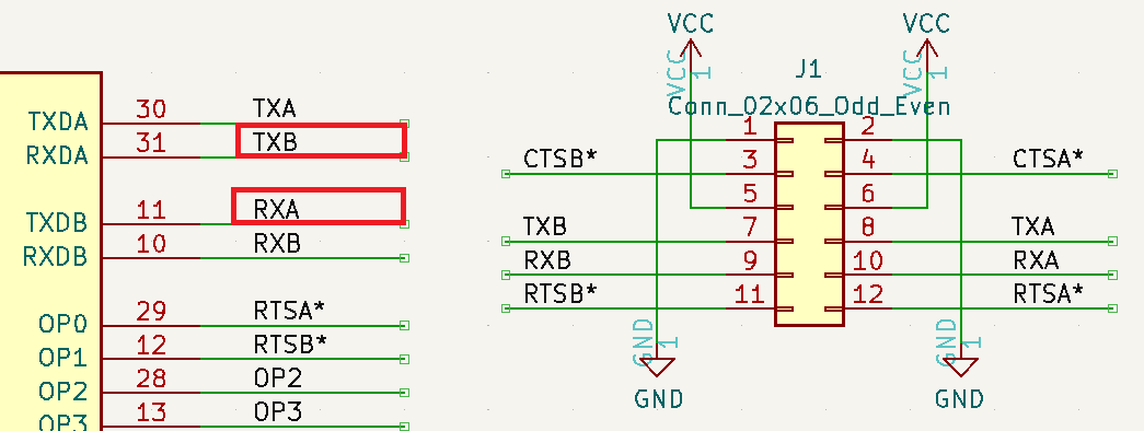
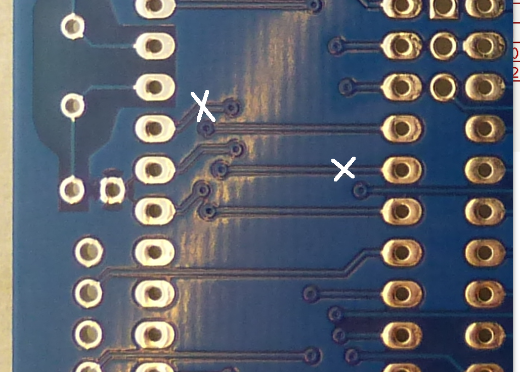
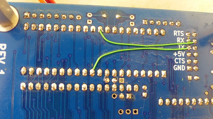
- Serial transmit/receive lines swapped
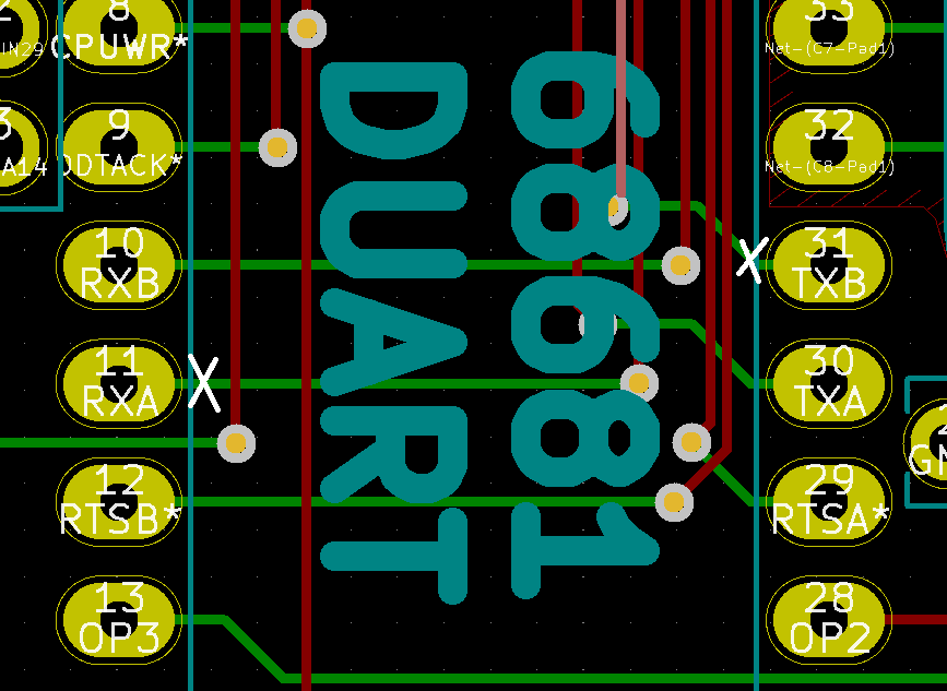
- TXB and RXA are swapped on DUART
- U6 pins 11 and 31 need to be swapped
- Easiest cuts (on bottom of board)
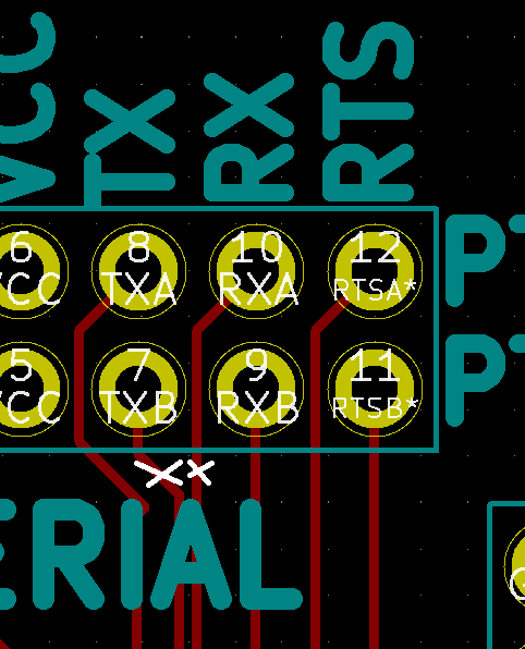
- Cuts as seen from the top side Silkscreen
- 2 Jumpers
- Alternative cut (harder due to space and being on top of board)
Assembly Sheet
Rev 2
Rev 1
Sockets
Mfr. #			Manufacturer		Customer #	Description
4848-6000-CP		3M			SKT_48_DIP	IC & Component Sockets 48P DUAL WIPE DIPSKT
1107741			Aries Electronics			IC & Component Sockets OSCILLATOR FULL 4PIN
110-44-632-41-001000	Mill-Max		SKT_32_DIP	IC & Component Sockets 32P TIN PIN TIN CONT
110-44-640-41-001000	Mill-Max		SKT_DIP-40	IC & Component Sockets 40P TIN PIN TIN CONT
110-99-320-41-001000	Mill-Max		SKT_20_DIP	IC & Component Sockets 20P TIN PIN TIN CONT
Part Substitutions
- EPROM on PL is nominal part number (27C040)
- I used Winbond W27C512 part from this ebay seller
- Ebay search for W27C512
- See sockets list below for quality machine contact sockets
- 48 pin socket is a dual wipe socket
